Monolithic integration structure of bulk acoustic wave resonator and capacitor, manufacturing method thereof, filter, duplexer and radio frequency communication module

A bulk acoustic wave resonator, bulk acoustic wave filter technology, applied in the direction of electrical components, impedance networks, etc., can solve the problems of reduced reliability of bulk acoustic wave filters, bulky bulk acoustic wave filters, bare chip and capacitor connection loss, etc. Achieve the effects of avoiding parasitic coupling effects, good roll-off characteristics, and enhanced roll-off characteristics

Active Publication Date: 2018-09-07
SUZHOU HUNTERSUN ELECTRONICS CO LTD
View PDF6 Cites 10 Cited by
  • Summary
  • Abstract
  • Description
  • Claims
  • Application Information

AI Technical Summary

Problems solved by technology

Although this method can enhance the roll-off characteristics of the bulk acoustic wave filter without deteriorating the passband performance of the bulk acoustic wave filter, since the capacitor is arranged outside the bare chip, it is necessary to provide additional support for the bulk acoustic wave resonator unit and the substrate of the capacitor. In this way, not only will the volu

Method used


Image

  • Monolithic integration structure of bulk acoustic wave resonator and capacitor, manufacturing method thereof, filter, duplexer and radio frequency communication module
  • Monolithic integration structure of bulk acoustic wave resonator and capacitor, manufacturing method thereof, filter, duplexer and radio frequency communication module
  • Monolithic integration structure of bulk acoustic wave resonator and capacitor, manufacturing method thereof, filter, duplexer and radio frequency communication module

Examples


no. 1 example

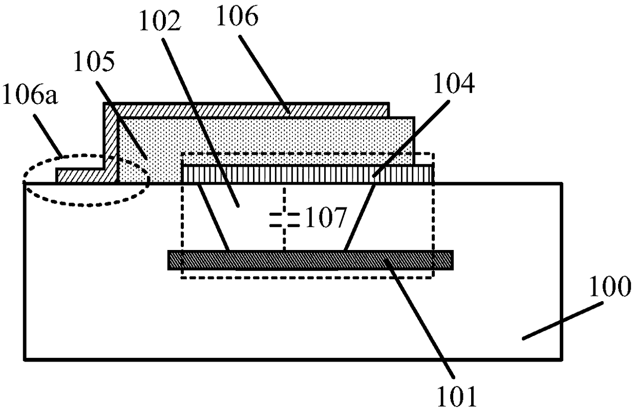
[0075] This embodiment provides a monolithic integrated structure of a bulk acoustic wave resonator and a capacitor, and the monolithic integrated structure of a bulk acoustic wave resonator and a capacitor includes:

[0076] Substrate;

[0077] a lower electrode, the lower electrode is disposed on the substrate and forms a cavity with the substrate;

[0078] a piezoelectric layer disposed on the lower electrode;

[0079] an upper electrode, the upper electrode is disposed on the piezoelectric layer;

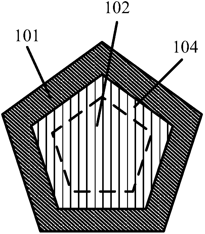
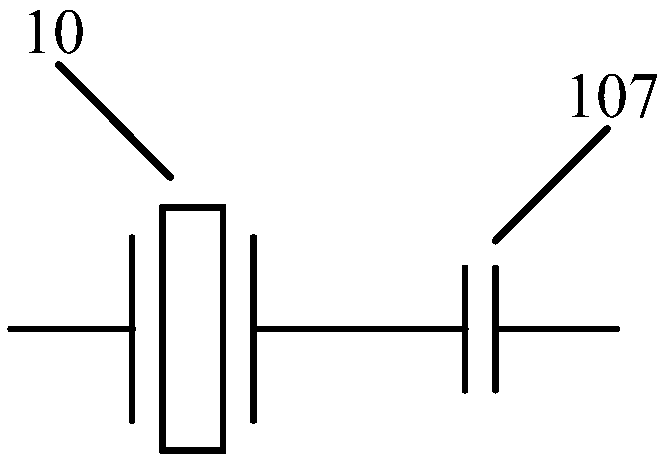
[0080] A first electrode, the first electrode is disposed in the substrate below the cavity and has a first overlapping area with the lower electrode.

[0081] Next, various parts of the monolithic integrated structure of the bulk acoustic wave resonator and capacitor provided by this embodiment will be described in detail with reference to FIG. 1( a ).

[0082] Specifically, as shown in FIG. 1( a ), the monolithic integrated structure of a bulk acoustic wave resonator and a ...

no. 2 example

[0087] This embodiment provides a monolithic integrated structure of a bulk acoustic wave resonator and a capacitor. This embodiment is basically the same as the first embodiment, the difference between the two mainly lies in that the monolithic integrated structure of the bulk acoustic wave resonator and the capacitor in this embodiment also includes a second electrode arranged on the upper surface of the substrate, Wherein, in addition to forming an overlapping area with the lower electrode, the first electrode also forms an overlapping area with the second electrode.

[0088] Next, the monolithic integrated structure of the bulk acoustic wave resonator and capacitor provided by this embodiment will be described with reference to FIG. 2( a ). For the sake of brevity, only the difference between this embodiment and the first embodiment will be described in detail below, and for the same parts between this embodiment and the first embodiment, please refer to the content descri...

no. 3 example

[0093] This embodiment provides a monolithic integrated structure of a bulk acoustic wave resonator and a capacitor. This embodiment is basically the same as the first embodiment, except that the first electrode not only forms an overlapping area with the lower electrode, but also forms a gap between the upper electrode and the part extending to the upper surface of the substrate. form overlapping regions.

[0094] Next, the monolithic integrated structure of the bulk acoustic wave resonator and capacitor provided by this embodiment will be described with reference to FIG. 3( a ). For the sake of brevity, only the difference between this embodiment and the first embodiment will be described in detail below, and for the same parts between this embodiment and the first embodiment, please refer to the content description of the corresponding part in the first embodiment.

[0095] Referring to FIG. 3( a ), the upper electrode 106 extends from the piezoelectric layer 105 to the up...


PUM

PropertyMeasurementUnit
Thicknessaaaaaaaaaa
Thicknessaaaaaaaaaa
Thicknessaaaaaaaaaa

Abstract

The invention provides a monolithic integration structure of a bulk acoustic wave resonator and a capacitor. The monolithic integration structure comprises: a substrate; a lower electrode, wherein thelower electrode is arranged on the substrate and forms a cavity with the substrate; a piezoelectric layer, wherein the piezoelectric layer is arranged on the lower electrode; an upper electrode, wherein the upper electrode is arranged on the piezoelectric layer; and a first electrode, wherein the first electrode is arranged in the substrate, is located below a hollow cavity and has a first overlapped area with the lower electrode. Correspondingly, the invention further provides a manufacturing method of the monolithic integration structure of the bulk acoustic wave resonator and the capacitor, a bulk acoustic wave filter, a duplexer and a radio frequency communication module. By implementation of the monolithic integration structure provided by the invention, the monolithic integration ofthe bulk acoustic wave resonator and the capacitor can be achieved, the bulk acoustic wave filter is formed by using the monolithic integration structure, thereby being not only able to ensure the roll-off features of the bulk acoustic wave filter, but also being able to effectively reduce the volume of the bulk acoustic wave filter, and thus the volumes of the duplexer and the radio frequency communication module are effectively reduced.

Description

technical field [0001] The invention relates to the technical field of electronic components, in particular to a monolithic integrated structure of a bulk acoustic wave resonator and a capacitor and a manufacturing method thereof, a bulk acoustic wave filter, a duplexer and a radio frequency communication module. Background technique [0002] With the advent of the 4G / LTE era, mobile phones need to work in more frequency bands and higher frequencies, which makes the RF front-end modules in mobile phones need to embed more filters and duplexers. At the same time, people have also put forward higher requirements for the portability and low power consumption of mobile phones. The bulk acoustic wave filter and duplexer composed of bulk acoustic wave (BAW, Bulk Acoustic Wave) resonators can well meet the needs of 4G / LTE mobile phones with small volume, low insertion loss and excellent roll-off characteristics. RF front-end filtering needs. [0003] For applications in specific ...

Claims


Application Information

Patent Timeline
IPC IPC(8): H03H9/02H03H9/54H03H9/70
CPCH03H9/02015H03H9/02047H03H9/02125H03H9/54H03H9/706
Inventor 蔡洵赖志国谢恒田晓洁赖亚明杨清华
Owner SUZHOU HUNTERSUN ELECTRONICS CO LTD
Why Eureka
Try Eureka