Substrate, flexible electronic component and manufacturing method of flexible electronic component
A technology for flexible electronic devices and electronic components, which is applied in the manufacture of extensible conductors/cables, extensible conductors, extensible conductor cables, etc. problem, to achieve the effect of improving tensile properties
- Summary
- Abstract
- Description
- Claims
- Application Information
AI Technical Summary
Problems solved by technology
Method used
Image
Examples
no. 1 approach
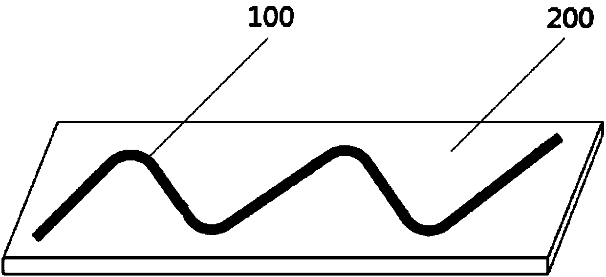
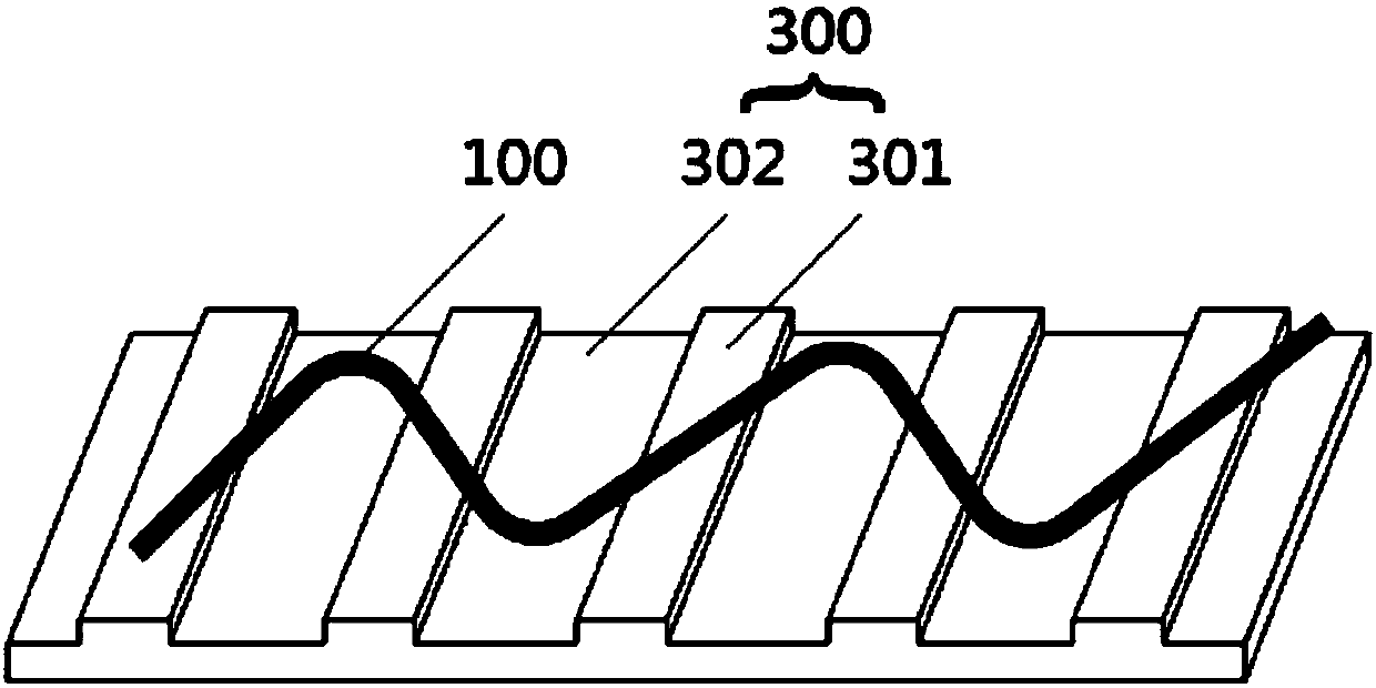
[0032] figure 2 The schematic three-dimensional structure of the flexible electronic component according to the first embodiment of the present invention is shown in , which is the interconnection wire and the corresponding base part of the flexible electronic device. figure 2 The left-right direction in is the lengthwise direction of the flexible electronic component, and in this embodiment, it is desired to improve the stretchability of the flexible electronic component in its lengthwise direction. Below, will figure 2 The left-right direction in is used as an example of "first direction".
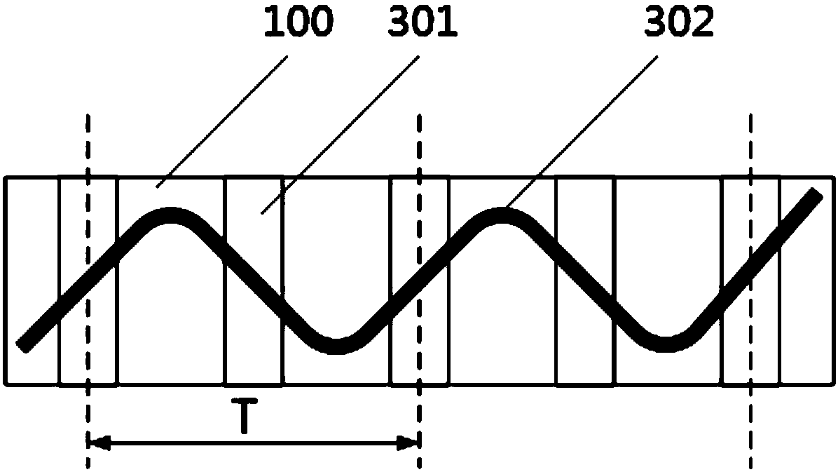
[0033] figure 2 The illustrated flexible electronic component includes interconnection wires 100 and a substrate 300 for carrying the interconnection wires 100 . The interconnection wire 100 is, for example, a wire made of metal, and the substrate 300 is, for example, a flexible substrate made of PDMS. The base 300 is provided with a plurality of bosses 301 arranged along the fir...
no. 2 approach
[0055] The present embodiment is a manufacturing method for manufacturing the flexible electronic component according to the first embodiment. Specifically, the manufacturing method of this embodiment includes the following steps: a base forming step, a wire manufacturing step, and a transfer printing step.
[0056] In the base forming step, the specific size of the base 300 is determined according to the first embodiment, and a mold corresponding to the base 300 is prefabricated, and the base 300 is cast in the mold.
[0057] In the wire manufacturing step, the specific size of the interconnection line 100 is determined according to the first embodiment, and the interconnection line 100 is prepared by means of, for example, a photolithography process.
[0058] In the transfer step, the interconnection 100 is transferred onto the substrate 300 by, for example, a transfer method.
[0059] The above-mentioned substrate forming step and lead manufacturing step are not in sequenc...
PUM
| Property | Measurement | Unit |
|---|---|---|
| Bump height | aaaaa | aaaaa |
Abstract
Description
Claims
Application Information


