
Shift register unit, driving method thereof, gate driving circuit and display device

A gate drive circuit and shift register technology, applied in static memory, digital memory information, instruments, etc., can solve problems such as abnormal signal output, poor display, etc., achieve the goal of reducing the number of transistors, improving the display effect, and reducing the threshold voltage drift effect

Active Publication Date: 2018-09-25
HEFEI XINSHENG OPTOELECTRONICS TECH CO LTD +1
View PDF5 Cites 13 Cited by
  • Summary
  • Abstract
  • Description
  • Claims
  • Application Information

AI Technical Summary

Problems solved by technology

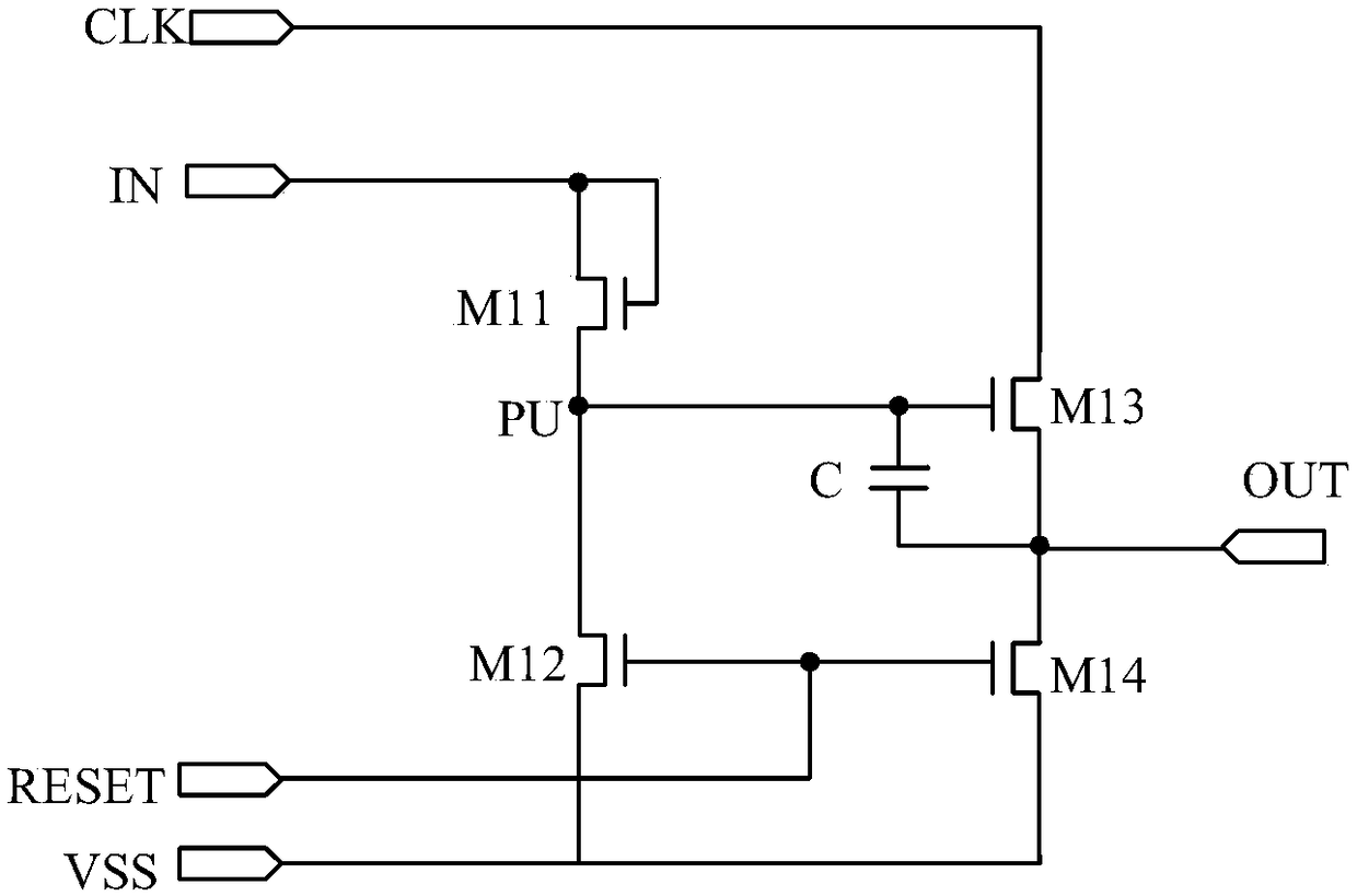
[0004] In the above process, the pull-up node PU will reach a higher potential due to the bootstrap effect of the capacitor C in the output stage, so that the third transistor M13 bears a higher gate bias voltage, resulting in the threshold voltage (Vth) of the third transistor M13 ) characteristics gradually drift, and when the drift reaches a certain level, the switching characteristics of the third transistor M13 will change, resulting in abnormal signal output and poor display

Method used


Image

  • Shift register unit, driving method thereof, gate driving circuit and display device
  • Shift register unit, driving method thereof, gate driving circuit and display device
  • Shift register unit, driving method thereof, gate driving circuit and display device

Examples


Embodiment Construction

[0069] Specific embodiments of the present invention will be described in detail below in conjunction with the accompanying drawings. It should be understood that the specific embodiments described here are only used to illustrate and explain the present invention, and are not intended to limit the present invention.

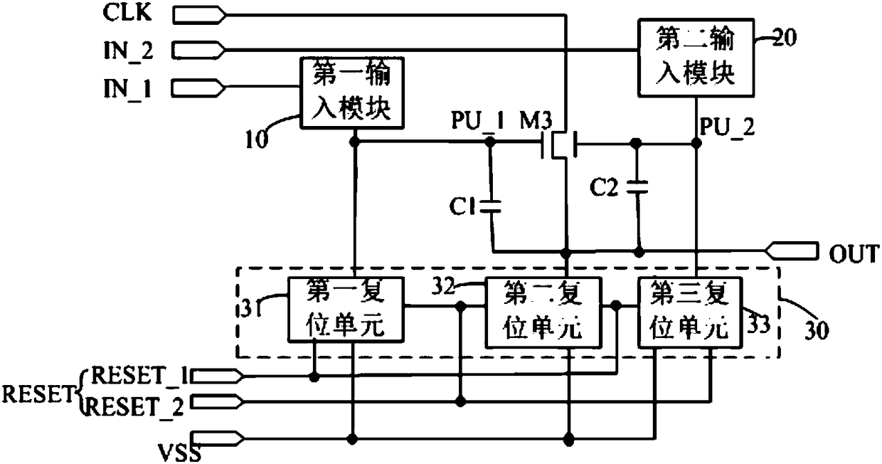
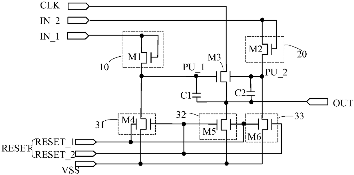
[0070] As an aspect of the present invention, a shift register unit is provided, such as figure 2 As shown, the shift register unit includes: a first input terminal IN_1, a second input terminal IN_2, a first pull-up node PU_1, a second pull-up node PU_2, a reset terminal RESET, a signal output terminal OUT, a clock signal terminal CLK, The invalid signal terminal VSS, the first input module 10 , the second input module 20 , the pull-up transistor M3 , the first capacitor C1 , the second capacitor C2 and the reset module 30 . Wherein, the first input module 10 is connected with the first input terminal IN_1 and the first pull-up node PU_1, and is used for cond...


PUM


Abstract

The invention provides a shift register unit, a driving method thereof, a gate driving circuit and a display device. The shift register unit comprises a first input terminal, a second input terminal,a first pull-up node, a second pull-up node, a reset terminal, a signal output terminal, a clock signal terminal, a first input module, a second input module, a pull-up transistor, a first capacitor,a second capacitor and a reset module, wherein the first input module is connected with first input terminal and the first pull-up node; the second input module is connected with the second input terminal and the second pull-up node; the pull-up transistor is a double-gate thin film transistor, the first gate of the double-gate thin film transistor is connected with the first pull-up node, the second gate is connected with the second pull-up node, one of the source and drain is connected with the clock signal terminal, and the other is connected with the signal output terminal; the first capacitor is connected between the first pull-up node and the signal output terminal; the second capacitor is connected between the second pull-up node and the signal output terminal; and the reset moduleis connected with the first pull-up node, the second pull-up node, the reset terminal and an invalid signal terminal. The shift register unit can reduce the threshold characteristic shift of the pull-up transistor.

Description

technical field [0001] The invention relates to the field of display technology, in particular to a shift register unit, a driving method thereof, a gate driving circuit and a display device. Background technique [0002] Gate On Array (GOA) technology is a process technology that integrates the gate drive circuit on the array substrate to replace the external drive chip. This technology has the characteristics of reducing production costs and production processes. has been widely used. The gate drive circuit includes a plurality of cascaded shift register units, each shift register unit corresponds to a row of gate lines, and the gate drive circuit sequentially provides scanning signals to each gate line in sequence during a display period of one frame of image. [0003] figure 1 Shown is a schematic structural diagram of the most basic shift register unit, which includes four thin film transistors and a capacitor. In the charging stage of the shift register unit, its in...

Claims


Application Information

Patent Timeline
Patent Type & Authority Applications(China)
IPC IPC(8): G09G3/20G11C19/28
CPCG09G3/20G11C19/28G09G3/3266G09G3/3677G11C19/184G09G2310/0267G09G2310/0286G09G3/2092G09G2300/0426G11C19/287
Inventor 张淼陈沫孙静傅武霞
Owner HEFEI XINSHENG OPTOELECTRONICS TECH CO LTD
Learn More