No-chip tag structure

A chip-free, label-free technology, applied to record carriers, instruments, and computer parts used in machines, can solve the problems of narrow occupied bandwidth and limited coding capacity, and achieves increasing the number of codes, realizing miniaturization, and coding density. high effect

Inactive Publication Date: 2018-10-09
BEIJING UNIV OF POSTS & TELECOMM
View PDF3 Cites 4 Cited by
  • Summary
  • Abstract
  • Description
  • Claims
  • Application Information

AI Technical Summary

Problems solved by technology

This encoding method occupies a narrow bandwidth, but the encoding capacity is limited

Method used


Image

  • No-chip tag structure
  • No-chip tag structure
  • No-chip tag structure

Examples


Embodiment Construction

[0026] In order to make the object, technical solution and advantages of the present invention clearer, the present invention will be described in further detail below in conjunction with specific embodiments and with reference to the accompanying drawings.

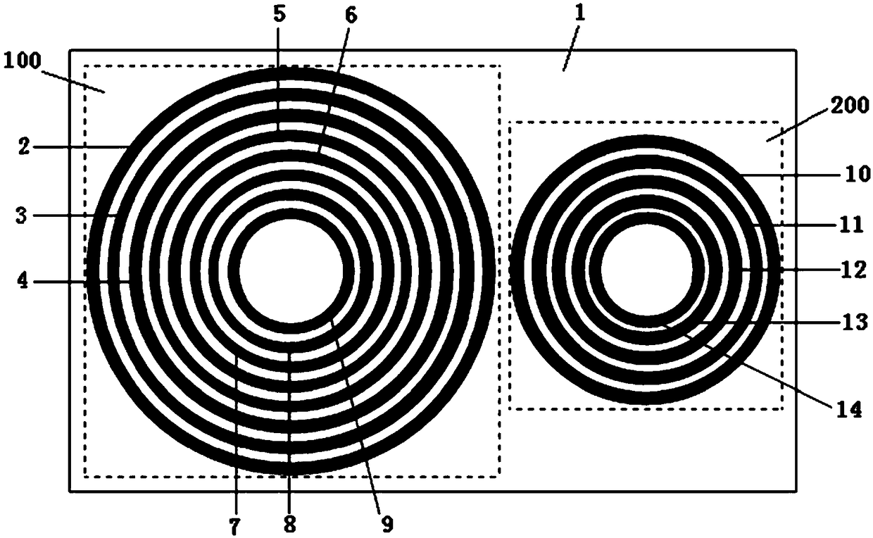
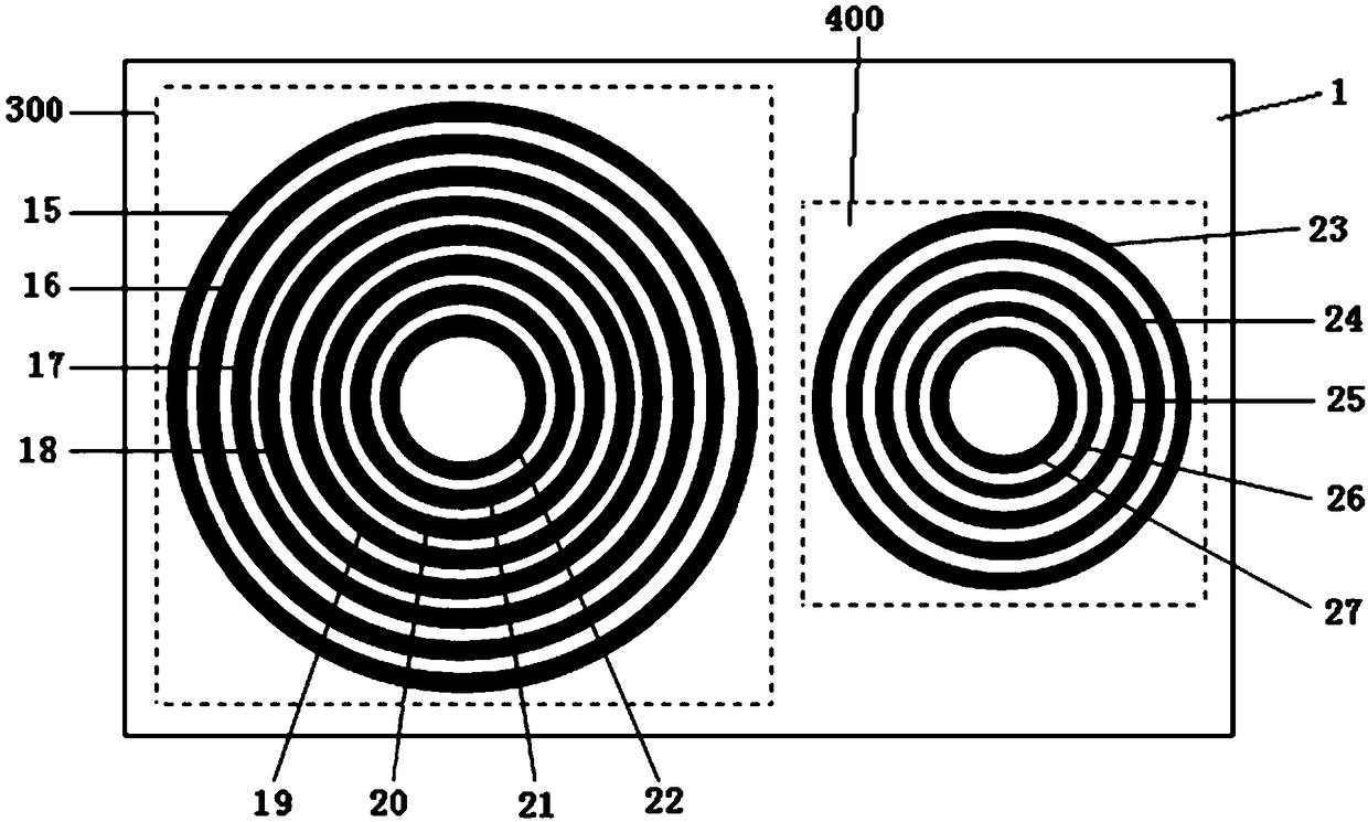
[0027] An embodiment of the present invention provides a chipless label structure, including: a dielectric plate, at least one multi-ring nested patch unit is provided on the surface of the dielectric plate; the multi-ring nested patch unit includes: a plurality of concentric Set of circular patches with different inner and outer radii. Preferably, the dielectric board is made of epoxy resin copper-clad laminate FR-4 board; the material of the ring patch is copper.

[0028] Wherein, the surface of the medium board includes an upper surface and a lower surface. One or more multi-ring nested patch units can be arranged on any one of the upper surface or the lower surface, or on both the upper surface and the lower surface....


PUM


Abstract

The invention discloses a no-chip tag structure, and the structure comprises a dielectric plate, wherein the surface of the dielectric plate is provided with at least one multi-ring nested paster unit. The multi-ring nested paster unit comprises a plurality of concentric annular pasters with different internal diameters and different external diameters. The structure provided by the invention aimsat the problems existing in the prior art, and the surface of the dielectric plate is flexibly provided with the multi-ring nested paster unit. The structure is small in size, is low in cost, is large in code capacity, and is high in code density.

Description

technical field [0001] The invention relates to the technical field of radio frequency identification electronic tags, in particular to a chipless tag structure. Background technique [0002] With the development of radio communication, the demand for tracking and positioning and target identification is gradually increasing. In short-distance or indoor communication environments, radio frequency identification technology is widely used. Radio Frequency Identification (RFID for short) refers to the technology that radio frequency signals transmit information through energy propagation, automatically identify target objects and obtain useful data. [0003] In RFID technology, tags have the advantages of long life, small size, large capacity, and reusability. However, due to the high cost of the label, its commercial production is very limited. A common label usually includes two parts, the antenna and the chip. The chip is the main source of the cost of the entire label. Re...

Claims


Application Information

Patent Timeline
Patent Type & Authority Applications(China)
IPC IPC(8): G06K19/077
CPCG06K19/0772G06K19/07749
Inventor 李秀萍朱华宋佳
Owner BEIJING UNIV OF POSTS & TELECOMM
Why Eureka
Try Eureka