Array substrate, display device and driving method thereof

An array substrate and sub-pixel technology, applied to static indicators, instruments, electrical components, etc., can solve problems such as unsatisfactory compensation effects and inaccurate signals

Active Publication Date: 2018-10-12
BOE TECH GRP CO LTD
View PDF7 Cites 33 Cited by
  • Summary
  • Abstract
  • Description
  • Claims
  • Application Information

AI Technical Summary

Problems solved by technology

[0005] Embodiments of the present invention provide an array substrate, a display device and a driving method thereof, which can improve the problem in t...

Method used


Image

  • Array substrate, display device and driving method thereof
  • Array substrate, display device and driving method thereof
  • Array substrate, display device and driving method thereof

Examples


Embodiment Construction

[0049] The following will clearly and completely describe the technical solutions in the embodiments of the present invention with reference to the accompanying drawings in the embodiments of the present invention. Obviously, the described embodiments are only some, not all, embodiments of the present invention. Based on the embodiments of the present invention, all other embodiments obtained by persons of ordinary skill in the art without making creative efforts belong to the protection scope of the present invention.

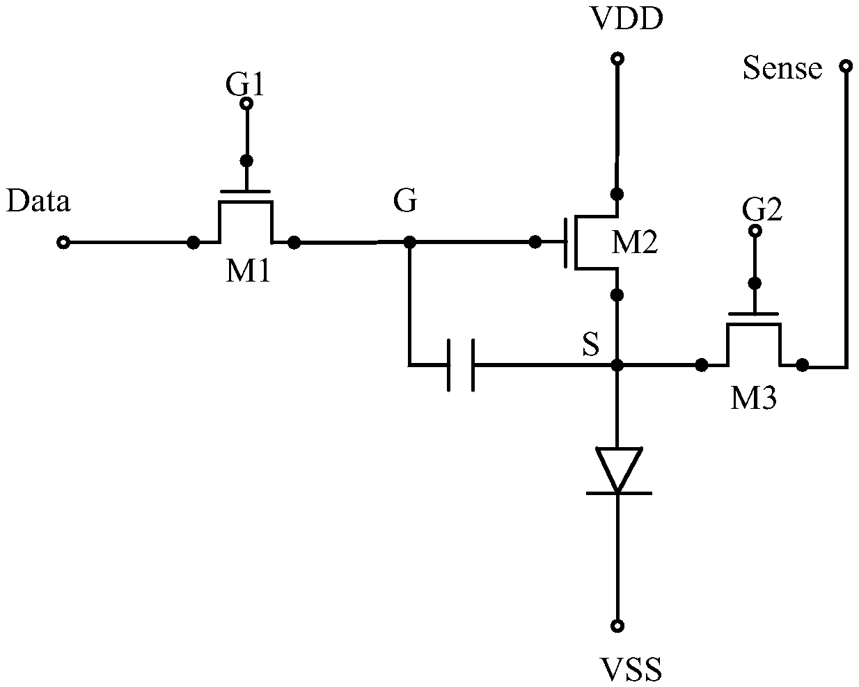
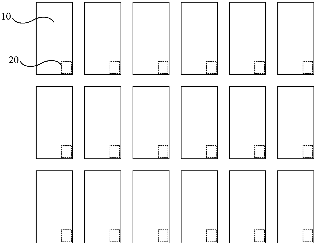
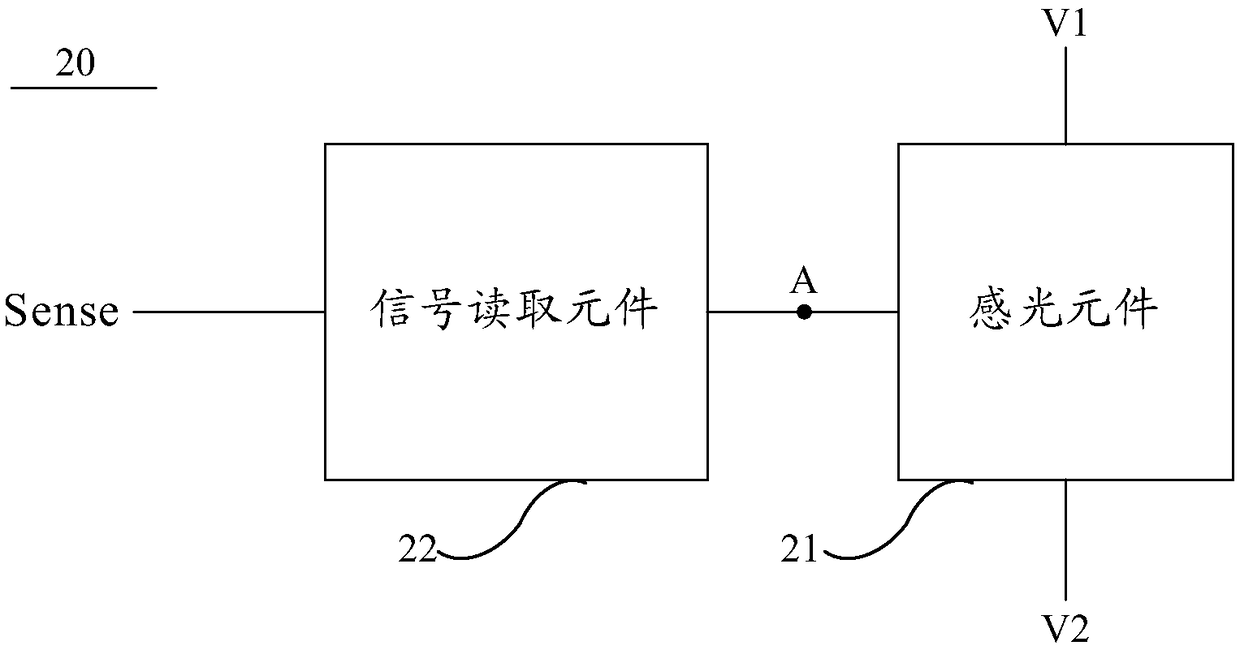
[0050] An embodiment of the present invention provides an array substrate, such as figure 2 As shown, it includes a plurality of sub-pixels 10, and each sub-pixel 10 is correspondingly provided with a photosensitive detection component 20, as image 3 As shown, the photosensitive detection component 20 includes a photosensitive element 21 and a signal reading element 22 .

[0051] The photosensitive element 21 is connected to the first voltage terminal V1 an...


PUM


Abstract

The present invention provides an array substrate, a display device and a driving method thereof, relates to the technical field of display, and can improve the problem that the compensation signal isnot accurate due to the inaccuracy of the signal received on the detection IC due to the weak compensation signal in the prior art. The array substrate comprises a plurality of sub-pixels; each of the sub-pixels is correspondingly provided with a photo-sensing detecting component, the photo-sensing detecting component comprises a photosensitive element and a signal reading element, the photosensitive component is connected to a first voltage end and a second voltage end and used for detecting the luminance of the sub-pixel and transmitting an electrical signal corresponding to the luminance of the sub-pixel to an output end of the photosensitive element, the signal reading element is also is connected to the output end and a signal reading line, and used for reading an electrical signal output by the output end and transmitting the electrical signal to the signal reading line; and wherein the sub-pixels at least partially correspond to the photosensitive elements in the photo-sensingdetecting components arranged correspondingly to the sub-pixels.

Description

technical field [0001] The present invention relates to the field of display technology, in particular to an array substrate, a display device and a driving method thereof. Background technique [0002] Organic Light Emitting Diode (OLED) display is one of the hotspots in the current research field. Compared with Liquid Crystal Display (LCD), OLED has low energy consumption, self-illumination, wide viewing angle and fast response speed. Etc. [0003] However, due to the process, materials and design of OLED display devices, it is easy to cause the threshold voltage of the driving thin film transistor to drift and the mobility (electron mobility) to fluctuate, resulting in different driving currents and uneven brightness of the display screen. . [0004] Based on this, in the prior art, an electrical compensation method is usually used to compensate for threshold voltage drift and mobility fluctuation, so as to ensure the uniformity of the driving current. Compensation cir...

Claims


Application Information

Patent Timeline
IPC IPC(8): H01L27/32
CPCH10K59/60H10K59/12G09G3/3233G09G2320/0233G09G2320/0295G09G2320/045G09G2360/148H10K59/351H10K59/13H10K59/1213G09G3/325G09G3/3266G09G3/3291G09G2300/0842H10K59/131
Inventor 王鹏鹏王海生丁小梁刘伟李昌峰韩艳玲张平
Owner BOE TECH GRP CO LTD
Why Eureka
Try Eureka