Manufacturing method of printed circuit board and printed circuit board

A printed circuit board and manufacturing method technology, applied in the directions of printed circuit manufacturing, printed circuit, multilayer circuit manufacturing, etc., can solve the problems of uneven force, incomplete back drilling, and difficult processing, so as to reduce damage and improve The effect of reliability and service life

Active Publication Date: 2020-08-07
NEW FOUNDER HLDG DEV LLC +1
View PDF3 Cites 0 Cited by
  • Summary
  • Abstract
  • Description
  • Claims
  • Application Information

AI Technical Summary

Problems solved by technology

[0003] However, there are still many disadvantages in the back drilling process.
For example, the uneven thickness of the board makes it difficult to process, and it is difficult to accurately control the depth; the back drilling is not thorough, and the residual copper skin will still affect the signal transmission quality; there is a risk of drilling through the conduction layer, and the product yield is greatly affected by it. Large; back drilling will cause semi-destructive structure to the hole, so that the hole will be unevenly stressed in the environment affected by thermal stress such as reflow soldering, which will easily cause the reliability failure of the local position

Method used


Image

  • Manufacturing method of printed circuit board and printed circuit board
  • Manufacturing method of printed circuit board and printed circuit board
  • Manufacturing method of printed circuit board and printed circuit board

Examples


Embodiment Construction

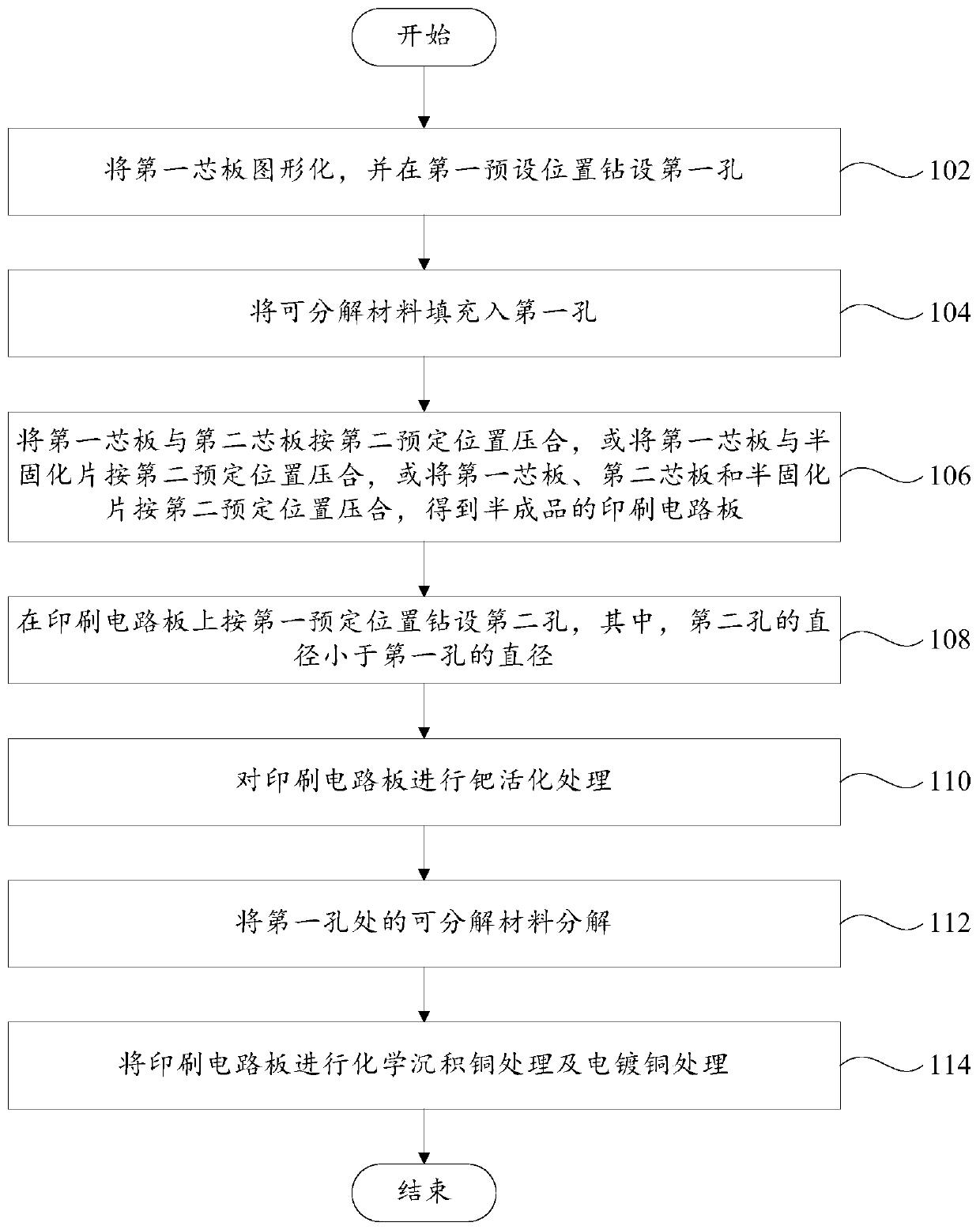
[0045] In order to understand the above-mentioned purpose, features and advantages of the present invention more clearly, the present invention will be further described in detail below in conjunction with the accompanying drawings and specific embodiments. It should be noted that, in the case of no conflict, the embodiments of the present application and the features in the embodiments can be combined with each other.

[0046] In the following description, many specific details are set forth in order to fully understand the present invention. However, the present invention can also be implemented in other ways different from those described here. Therefore, the protection scope of the present invention is not limited by the specific details disclosed below. EXAMPLE LIMITATIONS.

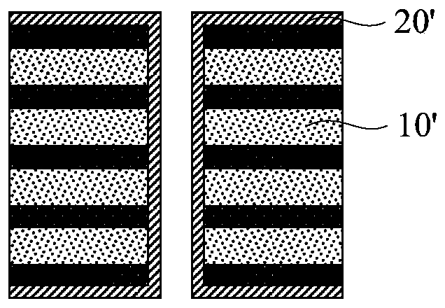
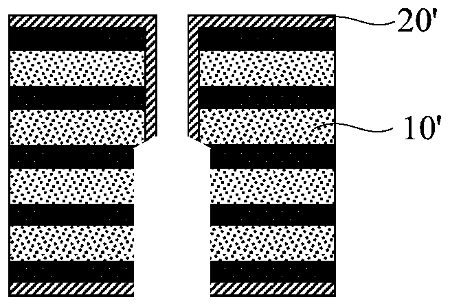
[0047] Refer below image 3 and Figure 13 A method of manufacturing the printed circuit board and the printed circuit board according to some embodiments of the present invention are described.

[...


PUM


Abstract

The present invention provides a manufacturing method of a printed circuit board and a printed circuit board. According to the manufacturing method of the printed circuit board, after a first core board is patternized, a first hole is formed at the predetermined position of the first core board by means of drilling; the first hole is filled with a decomposable material; the first core board and the other core board are laminated, and a second hole is formed at the same position with the first hole; the diameter of the first hole is larger than the diameter of the second hole, so that after thedrilling of the second hole is completed, the decomposable material is still left on the hole wall of the first core boar, and therefore, palladium can be deposited on the decomposable material afterpalladium activation treatment is carried out in a PTH process; and after the decomposable material is decomposed, the palladium is removed, so that a copper layer cannot be formed on the surface ofthe hole wall of the first core board during copper deposition and copper electroplating.

Description

technical field [0001] The invention relates to the technical field of printed circuit boards, in particular to a method for manufacturing a printed circuit board and the printed circuit board. Background technique [0002] At present, with the development of communication technology, communication electronic products have higher and higher requirements for signals. The update of each generation of products requires the technical support of the printed circuit board process, and it also poses a huge challenge to the printed circuit board industry. In the through-hole design of the printed circuit board, there are often some redundant paths that are invalid for signal transmission, and these paths have a significant impact on signal loss. In related technologies, such as figure 1 and figure 2 As shown, in order to solve such problems of the printed circuit board 10', the copper skin 20' on the invalid path in the through hole is mainly cut off by back drilling, so as to r...

Claims


Application Information

Patent Timeline
Patent Type & Authority Patents(China)
IPC IPC(8): H05K3/46H05K3/00
CPCH05K3/0088H05K3/4611H05K2203/12
Inventor 唐耀黄云钟
Owner NEW FOUNDER HLDG DEV LLC
Why Eureka
Try Eureka