Method and device for repairing semiconductor chips

A semiconductor and chip technology, applied in the field of semiconductor chip repairing methods and semiconductor chip repairing devices, can solve the problem that light-emitting diode chips can no longer be repaired and the like

Active Publication Date: 2018-11-02
STROKE PRECISION ADVANCED ENG CO LTD
View PDF6 Cites 11 Cited by
  • Summary
  • Abstract
  • Description
  • Claims
  • Application Information

AI Technical Summary

Problems solved by technology

However, in the prior art, when the LED chip fixed on the circuit substrate is damaged, the damaged LED chip cannot be repaired any more.

Method used


Image

  • Method and device for repairing semiconductor chips
  • Method and device for repairing semiconductor chips
  • Method and device for repairing semiconductor chips

Examples


Embodiment Construction

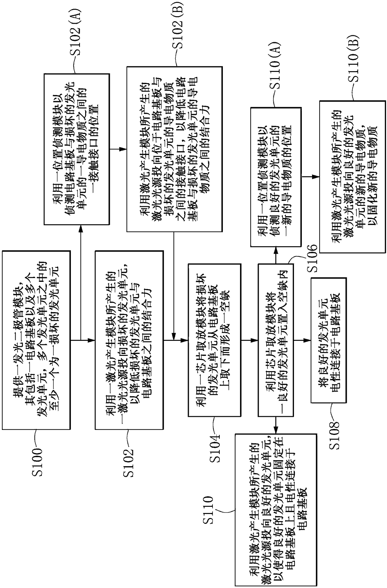
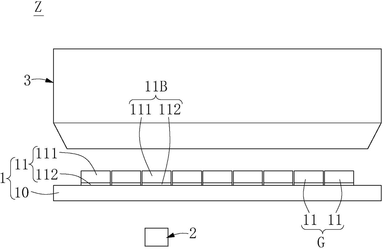
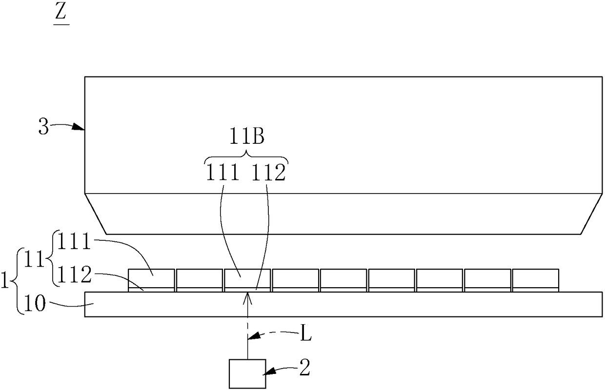
[0025] The following are specific examples to illustrate the implementation of the "semiconductor chip repair method and semiconductor chip repair device" disclosed in the present invention. Those skilled in the art can understand the advantages and effects of the present invention from the content disclosed in this specification. The present invention can be implemented or applied through other different specific embodiments, and various modifications and changes can be made to the details in this specification based on different viewpoints and applications without departing from the concept of the present invention. In addition, the drawings of the present invention are only for simple illustration, and are not drawn according to the actual size, which is stated in advance. The following embodiments will further describe the relevant technical content of the present invention in detail, but the disclosed content is not intended to limit the protection scope of the present inv...


PUM


Abstract

The present invention provides a method and a device for repairing semiconductor chips. The method includes providing an LED module that includes a circuit substrate and a plurality of light-emittingunits disposed on the circuit substrate, at least one of the light-emitting units being a bad light-emitting unit; projecting a laser light source generated by a laser generating module onto the bad light-emitting unit so as to decrease the bonding strength between the bad light-emitting unit and the circuit substrate; removing the bad light-emitting unit from the circuit substrate by a chip pick-and-place module so as to form a vacancy; placing a good light-emitting unit inside the vacancy by the chip pick-and-place module; and then electrically connecting the good light-emitting unit to thecircuit substrate. Therefore, the bad light-emitting unit can be replaced by the good light-emitting unit so as to achieve the repair effect.

Description

technical field [0001] The invention relates to a chip repair method and a chip repair device, in particular to a semiconductor chip repair method and a semiconductor chip repair device. Background technique [0002] Currently, light-emitting diodes (Light-Emitting Diodes, LEDs) are widely used due to their good light quality and high luminous efficiency. Generally speaking, in order to make the display device using light-emitting diodes as light-emitting components have better color performance capabilities, the prior art uses red, green and blue light-emitting diode chips to form a full-color light-emitting diode chip. Display equipment, this full-color light-emitting diode display device can emit red, green, and blue three-color light through red, green, and blue light-emitting diode chips, and then form a full-color light after mixing light. to display relevant information. However, in the prior art, when the LED chip fixed on the circuit substrate is damaged, the dama...

Claims


Application Information

Patent Timeline
Patent Type & Authority Applications(China)
IPC IPC(8): H01L33/48H01L33/62
CPCH01L33/48H01L33/62H01L2933/0066H01L2933/0033H01L33/0095H01L25/0753H01L25/50
Inventor 廖建硕
Owner STROKE PRECISION ADVANCED ENG CO LTD
Why Eureka
Try Eureka