Output driving circuit

A technology for outputting drive circuits and output stages, applied to electrical components, electronic switches, generating electrical pulses, etc., can solve problems such as high cost and large quantities

Active Publication Date: 2018-11-02
EVERDISPLAY OPTRONICS (SHANGHAI) CO LTD
View PDF11 Cites 7 Cited by
  • Summary
  • Abstract
  • Description
  • Claims
  • Application Information

AI Technical Summary

Problems solved by technology

[0005] All of these existing solutions use a large number of components as the structure of the front-end drive circuit. Those with ordinary knowledge in the industry know that a large number of components will directly increase the area of ​​the layout, especially in the casting process. A large number of photomasks are required in the wafer preparation stage, resulting in high cost

Method used


Image

  • Output driving circuit
  • Output driving circuit
  • Output driving circuit

Examples


Embodiment Construction

[0023] Below in conjunction with each embodiment, the technical solution of the present invention is clearly and completely set forth, but described embodiment is only the embodiment that the present invention is used for describing description and not all embodiments, based on these embodiments, this invention The solutions obtained by those skilled in the art without creative work all belong to the protection scope of the present invention.

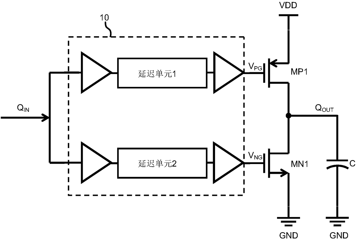
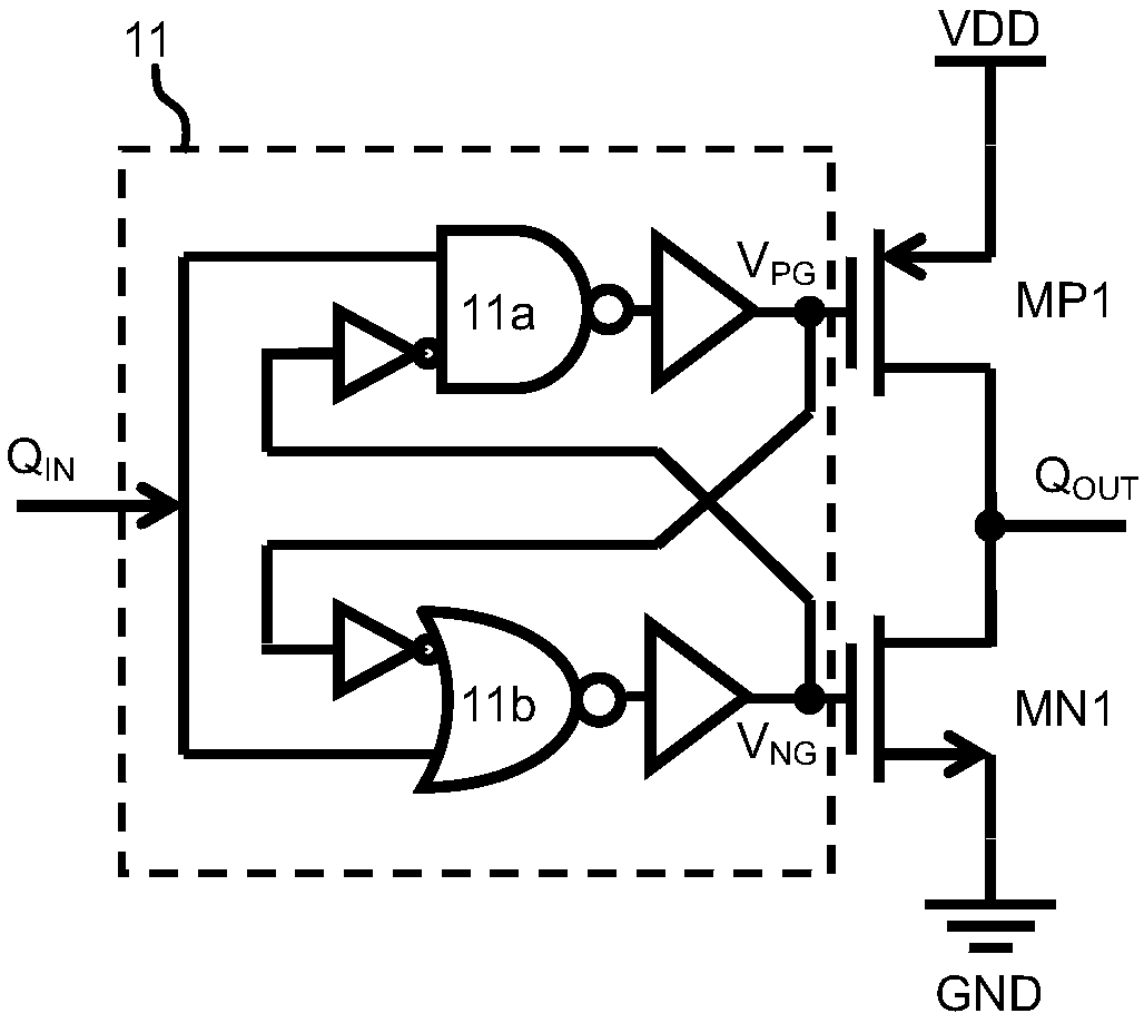
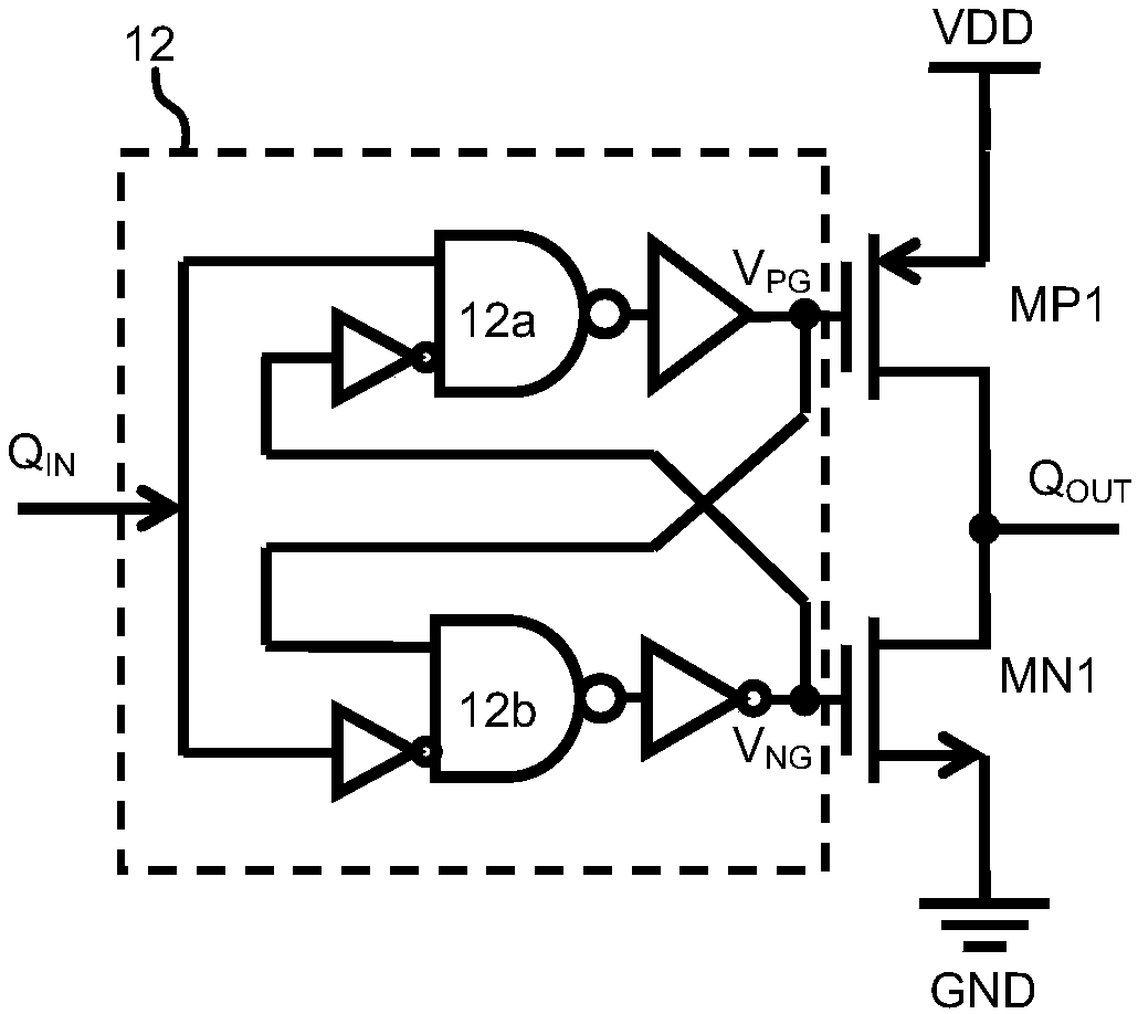
[0024] In order to have a deeper understanding of the spirit of the invention of this application, we first explain Figure 1 to Figure 3 The traditional implementation that uses more components and parts can realize the delay, and then compares the present invention with the Figure 4 A time-delay implementation that can greatly reduce the number of components is shown in .

[0025] see figure 1 , receiving an input signal Q IN The pre-stage driver 10 includes two control branches, the first control branch includes a delay unit 1 an...


PUM


Abstract

The invention mainly relates to a driver circuit for a semiconductor power switch, and designs an output driver circuit with a pre-stage driver. A first driving signal output by the pre-stage driver is used to drive a pull-up transistor at an output stage, a second driving signal output by the pre-stage driver is used to drive a pull-down transistor at the output stage, and the pre-stage driver isdesigned with a delay unit, so that complementary transistors at the output stage can be prevented from being simultaneously turned on in the phase of controlling the complementary transistors at theoutput stage.

Description

technical field [0001] The present invention is mainly concerned with driver circuits for semiconductor power switches, and more precisely, with the design of an output driver circuit with delay effects so that the output stage can be avoided during the control of the complementary transistor stages of the output stage. The complementary transistors are turned on simultaneously. Background technique [0002] In the driver circuit applied to semiconductor power switches, in order to obtain the maximum output power and minimize the power consumption of the transistor, the output stage transistor is usually driven by the control signal generated by the pre-stage driver, and performs complementary switching to drive the P-type transistor. and N-type transistors to avoid power loss caused by simultaneous conduction of P-type transistors and N-type transistors. Transistors connected directly in series between power and ground can cause irreversible thermal damage. [0003] Exist...

Claims


Application Information

Patent Timeline
Patent Type & Authority Applications(China)
IPC IPC(8): H03K3/356H03K17/687
CPCH03K3/356113H03K5/134H03K17/6872H03K2005/00215
Inventor 邹文安邱卫斌
Owner EVERDISPLAY OPTRONICS (SHANGHAI) CO LTD
Why Eureka
Try Eureka