Through-hole solder pad structure, circuit board connecting method and circuit board

A circuit board and pad technology, applied in the direction of electrical connection of printed components, printed circuits, printed circuits, etc., can solve the problems of board spacing, single arrangement, and space occupation.

Active Publication Date: 2018-11-13
北京华悦龙驰科技有限公司
View PDF8 Cites 1 Cited by
  • Summary
  • Abstract
  • Description
  • Claims
  • Application Information

AI Technical Summary

Problems solved by technology

When multiple circuit boards are connected, the layout is relatively simple,

Method used


Image

  • Through-hole solder pad structure, circuit board connecting method and circuit board
  • Through-hole solder pad structure, circuit board connecting method and circuit board
  • Through-hole solder pad structure, circuit board connecting method and circuit board

Examples


Embodiment 1

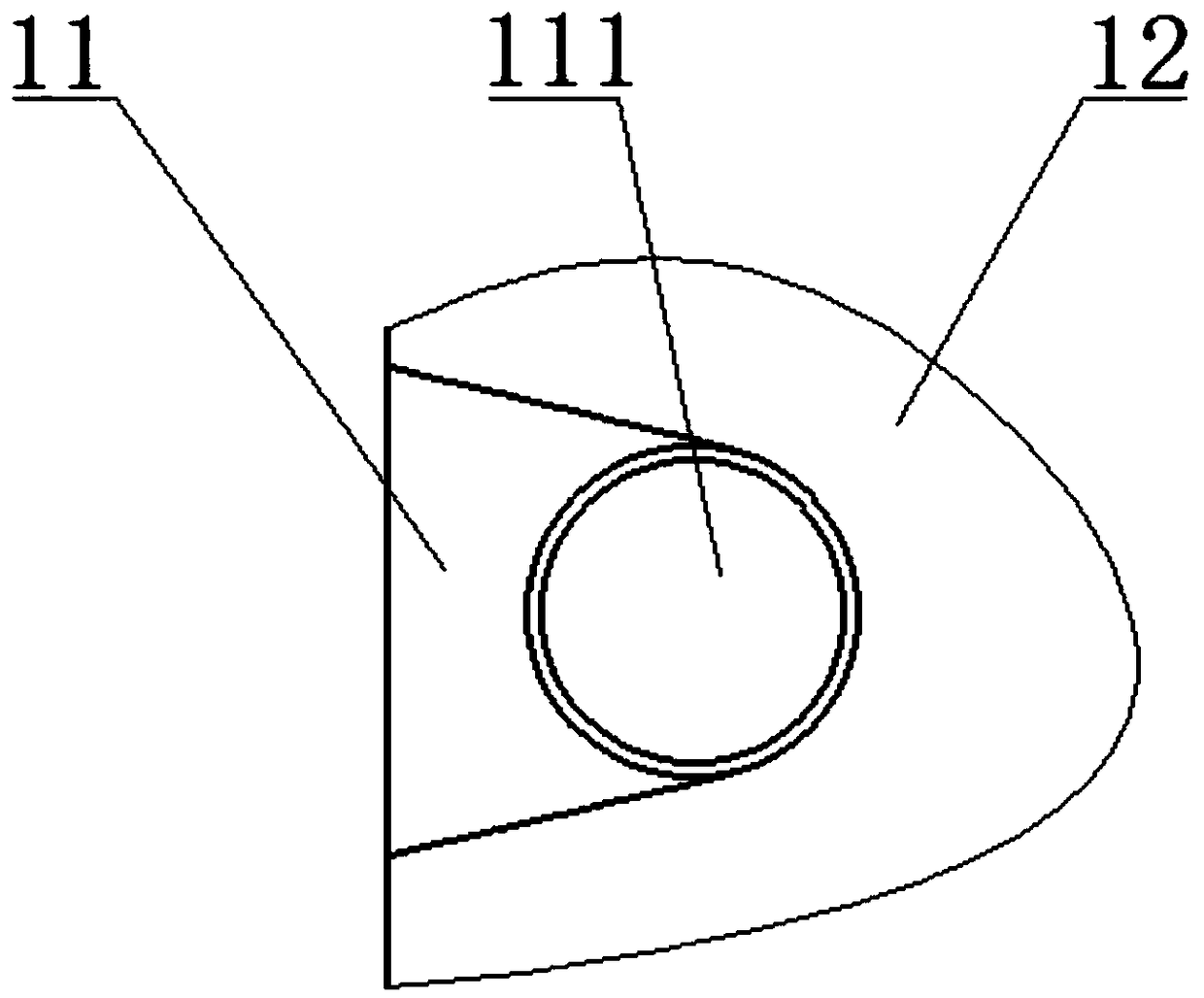
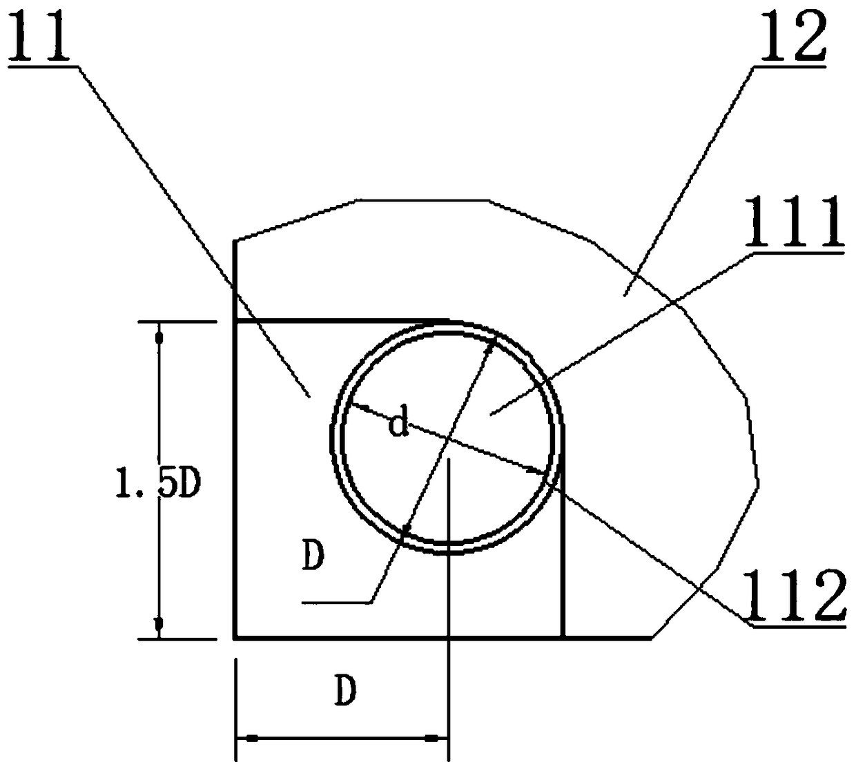
[0035] Such as figure 1 As shown, the edge position of the circuit board has a through hole pad structure, including a through hole 111 perpendicular to the board surface, and the position of the circuit board around the through hole includes a solder resist layer 12 arranged on the uppermost side, that is, the outermost side, and the solder resist layer 12 on the resister The solder layer 11 below the solder layer 12. Between the through hole 111 and its closest side, the solder resist layer 12 is removed to expose the solder layer 11 . The exposed surface of the soldering layer 11 is the soldering area, and the place outside the soldering area is the solder resist area.

[0036] The distance between the through hole 111 and the side of the circuit board is 1-1.5 times its diameter, and the width of the soldering area is not less than the diameter of the through hole 111 . The projected length of the welding area on the side preferably covers the projected length of the thr...

Embodiment 2

[0044] Such as Figure 4 As shown, S1, two circuit boards are taken, and through-hole pad structures are arranged at the corresponding positions on the sides;

[0045] S2, place the corresponding through-hole pad structure close to the board surface at a predetermined angle, which can be clamped with the help of tooling first;

[0046] S3: Reference Figure 5 , use solder to solder the lands of the two through-hole pad structures.

[0047] In the combined circuit board obtained by the method, the board surface angles of the two sub-circuit boards can be 90 degrees to 180 degrees. When the components on the board do not interfere, it can be an acute angle.

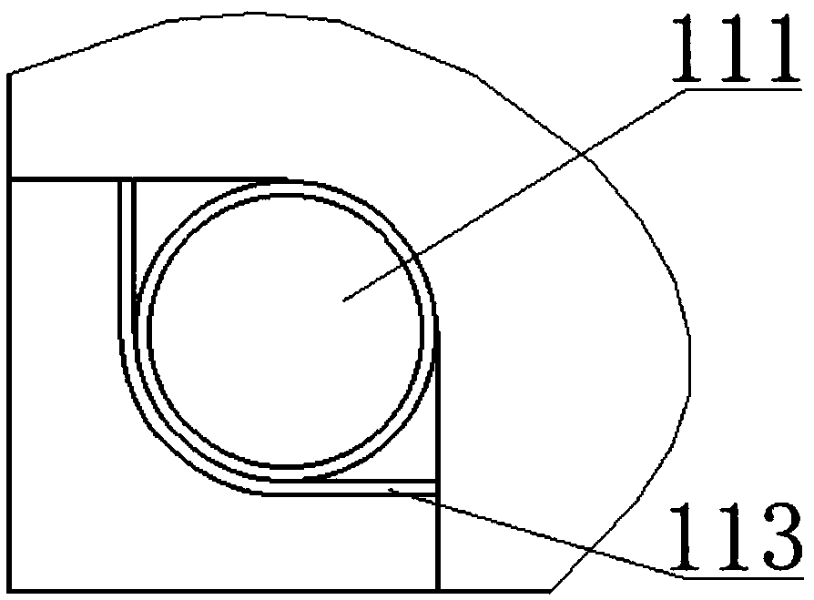
[0048] Such as Image 6 As shown, soldering areas are provided on both sides of the through hole 111, and both sides of the sub-circuit board can be used for soldering.

[0049] It is also possible to set a plurality of sub-circuit boards to be welded into a whole. Can be connected horizontally; can be T-shaped, two s...


PUM

PropertyMeasurementUnit
Widthaaaaaaaaaa

Abstract

The invention relates to a through-hole solder pad structure. The through-hole solder pad structure comprises a through hole perpendicular to a surface of a circuit board, and a distance between a center axis of the through hole to a side edge closest to the circuit board is 1 to 1.5 times of the diameter of the through hole; the circuit board on the periphery of the through hole comprises a solder mask layer on the outermost side and a solder layer on the inner side of the solder mask layer along the thickness direction; on the surface of the circuit board, the solder layer in an area betweenthe end part of the through hole and the side edge closest to the circuit board is exposed, and the exposed surface of the solder layer is a solder area; and the direction to which the through hole points the side edge closest to the circuit board is the length direction of the solder area, and a width of the solder area is not smaller than the diameter of the through hole. Based on the originalstructural design of the circuit board, the overall structure and shape of the circuit board are not changed, and the through-hole solder pad structure is used for flexibly connecting different circuit boards. The through-hole solder pad structure is diversified in use way, and suitable for installing the circuit board in a narrow space and a specially-shaped space.

Description

technical field [0001] The invention relates to the field of circuit boards, in particular to a circuit board connection method. [0002] The invention also relates to a through-hole pad structure and a circuit board. Background technique [0003] There are two main ways to connect existing circuit boards: one is to arrange pin headers and female headers on two circuit boards respectively, and then connect the pin headers and female headers. The pin header is used both for fixing and for signal connection. The connection of the pin header is mainly to realize the vertical stacking method and the horizontal docking method. There are also some special types of pin headers with a 90-degree angle, which can make the two boards form a 90-degree angle. But the height of the pin header is fixed, as long as the welded pin header is fixed, the distance between the two boards is fixed and cannot be changed. The pin header takes up a lot of space, and the model size is relatively fi...

Claims


Application Information

Patent Timeline
IPC IPC(8): H05K1/11
CPCH05K1/116H05K2201/09581
Inventor 李思奇
Owner 北京华悦龙驰科技有限公司
Why Eureka
Try Eureka