Preparation method of gallium nitride film layer and substrate

A thin-film, gallium nitride technology, used in semiconductor/solid-state device manufacturing, electrical components, circuits, etc., can solve the problem of reducing the utilization rate of epitaxial materials, large lattice mismatch and thermal mismatch, and expensive SiC substrates, etc. problem, to achieve the effect of good thermal conductivity, small lattice mismatch, and regular connection

Inactive Publication Date: 2014-05-14
BEIJING NAURA MICROELECTRONICS EQUIP CO LTD
View PDF3 Cites 16 Cited by
  • Summary
  • Abstract
  • Description
  • Claims
  • Application Information

AI Technical Summary

Problems solved by technology

[0004] However, there is a large lattice mismatch and thermal mismatch between the sapphire substrate and the gallium nitride material
Although the dislocation density inside the film can be reduced to a certain extent through patterned surface substrate technology and secondary growth methods, it is still difficult to control the quality of the film; When using photolithography, etching, evaporation and other complex processes to prepare electrodes on the epitaxial layer, this greatly reduces the effective light-emitting area and reduces the utilization of epitaxial materials; the low thermal conductivity of the sapphire substrate makes the heat dissipation of the device difficulty
[0005] Although the silicon carbide substrate has a low lattice mismatch rate with the gallium nitride material and has good thermal and electrical conductivity, it is necessary to grow AlGaN at a high temperature of about 1000 ° C as a conductive substrate before growing the gallium nitride thin film layer. core layer; and SiC substrates are expensive

Method used


Image

  • Preparation method of gallium nitride film layer and substrate
  • Preparation method of gallium nitride film layer and substrate
  • Preparation method of gallium nitride film layer and substrate

Examples


Embodiment Construction

[0048] In order to enable those skilled in the art to better understand the technical solution of the present invention, the method for preparing the gallium nitride thin film layer and the substrate provided by the present invention will be described in detail below with reference to the accompanying drawings.

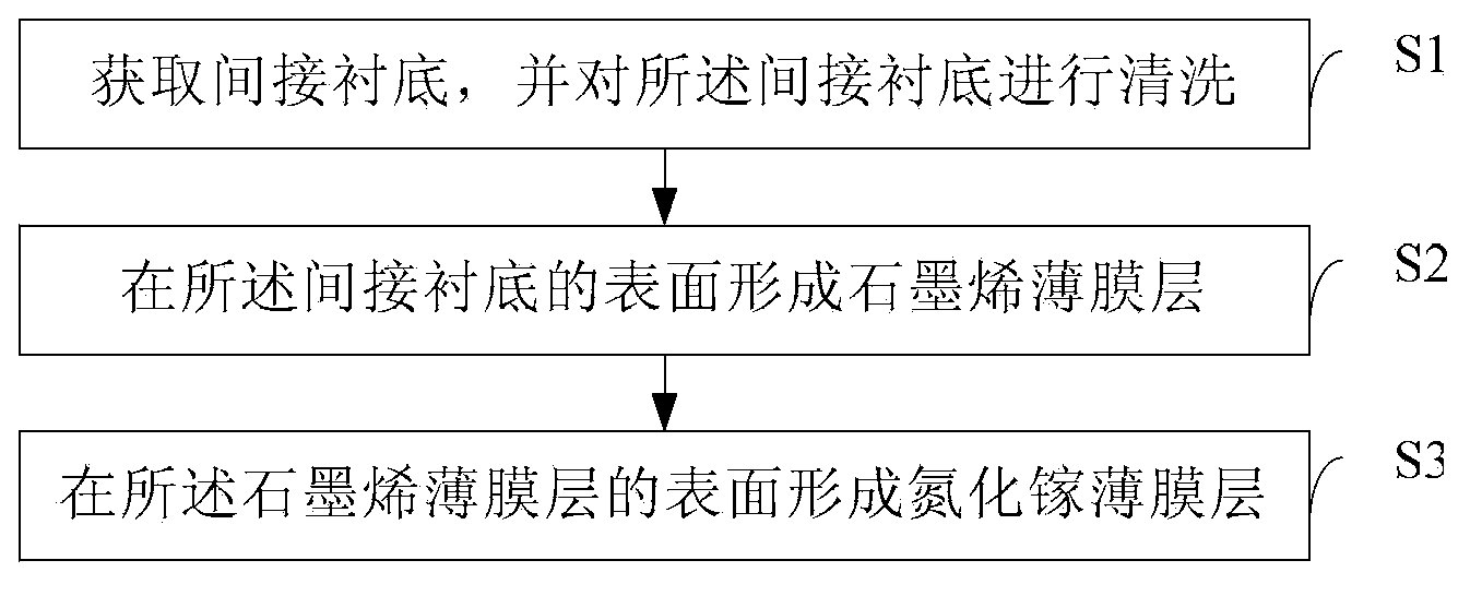
[0049] This embodiment provides a method for preparing a gallium nitride thin film layer. figure 1 It is a flowchart of a method for preparing a gallium nitride thin film layer according to an embodiment of the present invention. like figure 1 Shown, the preparation method of gallium nitride film layer comprises the following steps:

[0050] Step S1, obtaining an indirect substrate, and cleaning the indirect substrate.

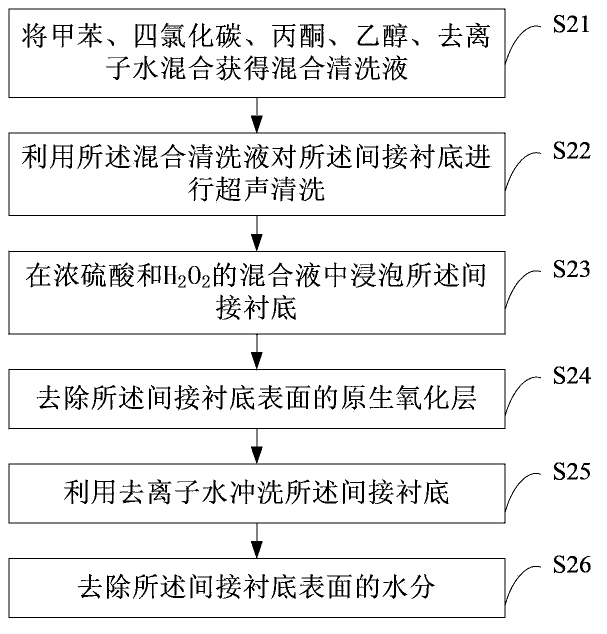
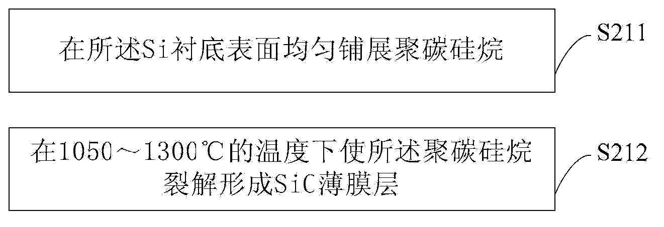
[0051] The indirect substrate can be sapphire substrate, SiC substrate, Si substrate, LiAlO 3 substrate or ZnO substrate. This embodiment takes the Si substrate as an example for illustration, as figure 2 Shown, the specific steps of cleaning Si...


PUM


Abstract

The invention provides a preparation method of a gallium nitride film layer and a substrate. The preparation method of the gallium nitride film layer comprises the following steps: obtaining and cleaning an indirect substrate; forming a graphene film on the surface of the indirect substrate; and forming a gallium nitride film layer on the surface of the graphene film. The preparation method of the gallium nitride film layer can effectively reduce the dislocation density of the gallium nitride film layer in a process of growth, thereby improving performance of the gallium nitride film layer.

Description

technical field [0001] The invention relates to a preparation method and a substrate of a gallium nitride thin film layer. Background technique [0002] Metal-organic Chemical Vapor Deposition (MOCVD for short) is a new type of vapor phase epitaxial growth technology developed on the basis of vapor phase epitaxial growth. It mainly uses organic compounds of group III and group II elements and V , hydrides of group VI elements, etc. as crystal growth source materials, perform vapor phase epitaxy on the substrate by thermal decomposition reaction, and grow thin-layer monolayers of various III-V, II-VI compound semiconductors and their multiple solid solutions crystal materials, such as GaN (gallium nitride) thin films commonly used in the semiconductor field. [0003] When using MOCVD to prepare gallium nitride thin films, the ideal substrate is a gallium nitride substrate that is homogeneous to gallium nitride thin films. GaN bulk single crystal is extremely difficult, ther...

Claims


Application Information

Patent Timeline
Patent Type & Authority Applications(China)
IPC IPC(8): H01L21/02
CPCH01L21/0254H01L21/02447
Inventor 涂冶
Owner BEIJING NAURA MICROELECTRONICS EQUIP CO LTD
Why Eureka
Try Eureka