A kind of manufacturing method of cmos thin film transistor and ltps array substrate

A technology of thin-film transistors and manufacturing methods, which is applied in the display field, can solve problems such as increased manufacturing costs, complex production processes, and large investment in equipment, and achieve the effects of reducing manufacturing costs, reducing the number of photomasks, and increasing production capacity

Active Publication Date: 2021-03-05
WUHAN CHINA STAR OPTOELECTRONICS TECH CO LTD
View PDF4 Cites 0 Cited by
  • Summary
  • Abstract
  • Description
  • Claims
  • Application Information

AI Technical Summary

Problems solved by technology

[0004] The above production process requires multiple photomask processes. Compared with the amorphous silicon process, the production process is more complicated, and the overall equipment investment is too large and the yield rate is too low, and the production cost increases accordingly. Therefore, how to effectively reduce the LTPS CMOS array The production cycle of substrates, improving production capacity and reducing costs are the focus of the current panel industry

Method used


Image

  • A kind of manufacturing method of cmos thin film transistor and ltps array substrate
  • A kind of manufacturing method of cmos thin film transistor and ltps array substrate
  • A kind of manufacturing method of cmos thin film transistor and ltps array substrate

Examples


Embodiment Construction

[0021] In order to make the purpose, technical solution and effect of the present application more clear and definite, the present application will be further described in detail below with reference to the accompanying drawings and examples.

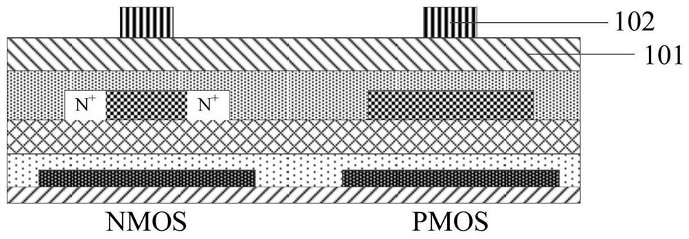
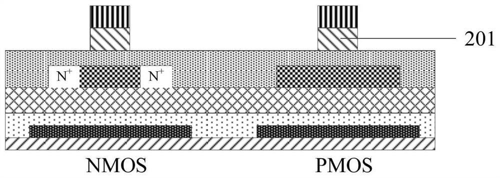
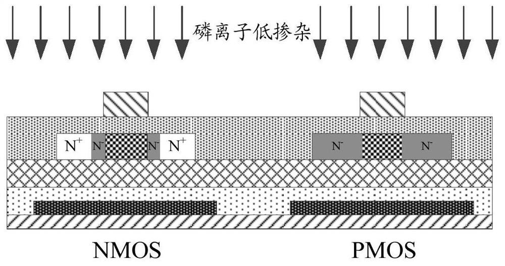
[0022] This application provides a method for manufacturing CMOS thin film transistors and LTPS array substrates. In this method, by changing the design of the mask, two doping processes can be realized with one mask process, which can reduce the number of masks in the manufacturing process. , shorten the production cycle, reduce the production cost, and increase the production capacity of the array substrate.

[0023] see Figure 5 , Figure 5 It is a schematic flow chart of the first embodiment of the manufacturing method of the CMOS thin film transistor of the present application. In this embodiment, the manufacturing method of the CMOS thin film transistor comprises the following steps:

[0024] S501: Provide a substrate, and seq...


PUM


Abstract

The invention discloses a manufacturing method of a CMOS thin film transistor and a manufacturing method of an LTPS array substrate; manufacturing method of the CMOS thin film transistor comprises thefollowing steps of providing a substrate, and sequentially forming an active layer, a gate layer and a photoresist layer on the substrate, wherein the active layer comprises a first region, a secondregion and a third region; patterning the photoresist layer by using a photomask, so that the second region is not covered by the photoresist layer, and the first region and the third region are covered by the remaining photoresist; performing first-degree doping on the second region; removing residual photoresist; and carrying out second-degree doping on the first region. By means of the mode, the number of the photo masks in the manufacturing process can be reduced, the manufacturing period is shortened, and the manufacturing cost is lowered.

Description

technical field [0001] The present application relates to the field of display technology, in particular to a method for manufacturing a CMOS thin film transistor and an LTPS array substrate. Background technique [0002] Thin-Film Transistor (TFT) technology can be divided into polysilicon (Poly-Si) technology and amorphous silicon (a-Si) technology, the difference between the two lies in the characteristics of transistors. Compared with traditional A-Si technology, Low Temperature Poly-Silicon (LTPS) technology is widely used in small and medium-sized high-resolution TFT LCDs and Fabrication of AMOLED panels. According to its production method, LTPS is mainly divided into N-type metal oxide semiconductor (Negative channel Metal Oxide Semiconductor, NMOS), P-type metal oxide semiconductor (Positive channel MetalOxide Semiconductor, PMOS) and complementary metal oxide semiconductor (Complementary Metal Oxide Semiconductor). , CMOS), where the main difference between NMOS t...

Claims


Application Information

Patent Timeline
Patent Type & Authority Patents(China)
IPC IPC(8): H01L21/77H01L27/12
CPCH01L27/1214H01L27/1288
Inventor 李立胜刘广辉李书晓
Owner WUHAN CHINA STAR OPTOELECTRONICS TECH CO LTD
Why Eureka
Try Eureka