Placement method for circuit carrier and circuit carrier
A technology for circuit carriers and equipment, which is applied in the direction of assembling printed circuits, circuits, printed circuits, etc. with electrical components, and can solve problems such as long process time and inaccurate positions
- Summary
- Abstract
- Description
- Claims
- Application Information
AI Technical Summary
Problems solved by technology
Method used
Image

Examples
Embodiment Construction
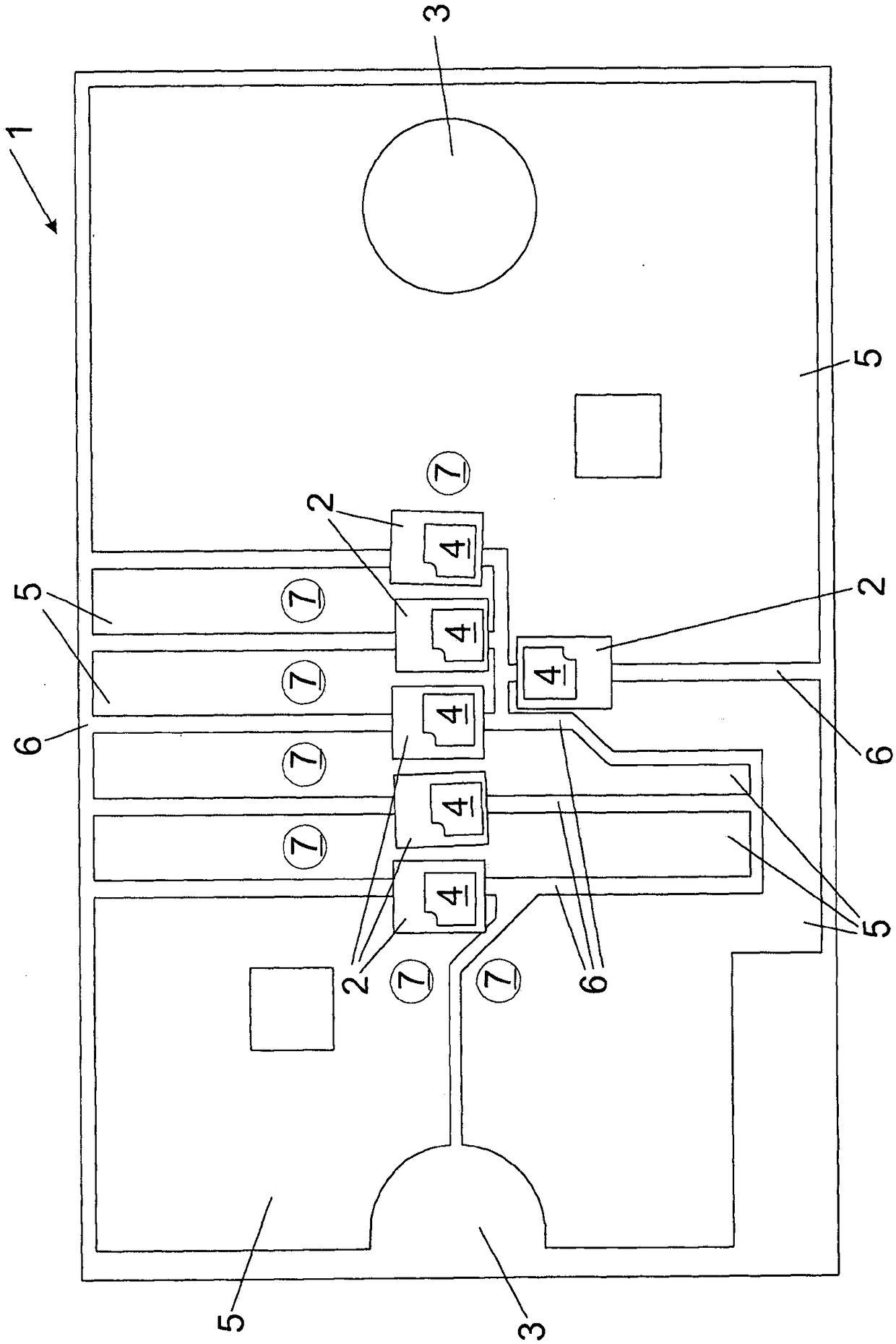
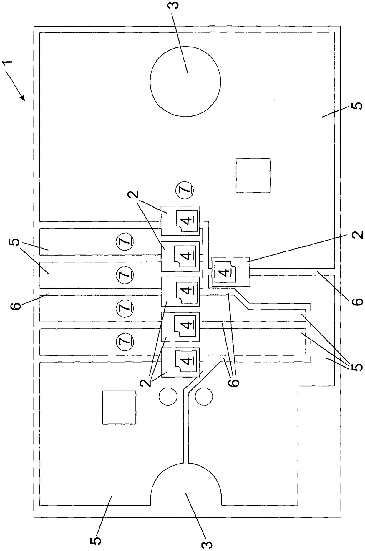
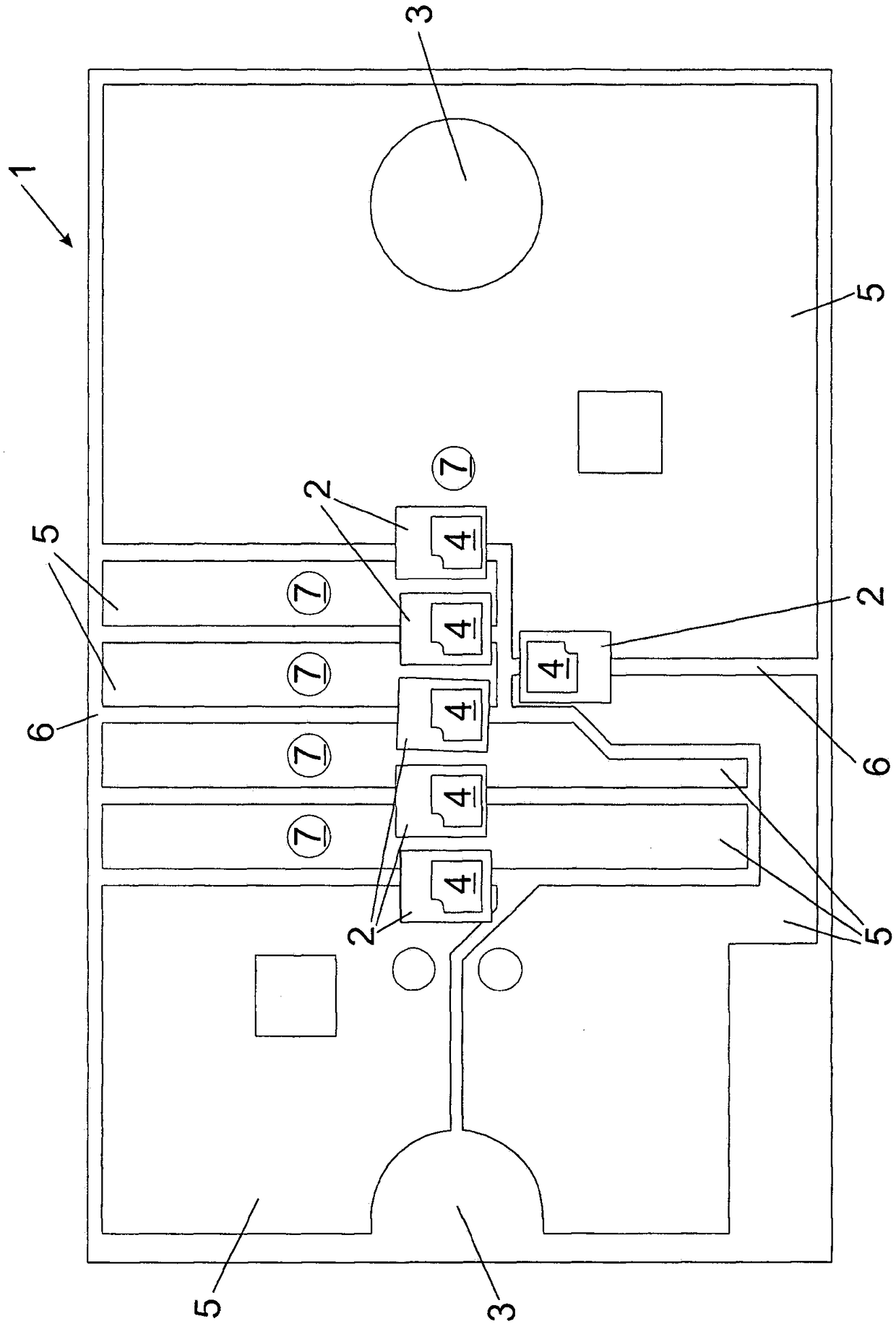
[0054] Figures 1 to 3 A test circuit diagram is shown for checking the positional accuracy of each individual SMD-LED2. The circuit carrier 1 has conductive surfaces 5 which are insulated from one another by insulating regions 6 . The conductive surface 5 can be supplied with electrical energy via a connection 7 .
[0055] figure 1 A circuit carrier 1 equipped with six SMD-LEDs 2 is shown. Two reference points 3 can be seen, which are used on the one hand to determine deviations in the defined position of the SMD-LED 2 on the circuit carrier 1 and on the other hand to fix a not shown position for the SMD-LED 2 optical system. The alignment of the optical system takes place via separate reference points, which are not shown in this figure.
[0056] exist figure 1 Assembly is carried out using "pick and place" and reflow soldering methods according to the prior art. The SMD-LED 2 is oriented with its outer contour relative to the reference point 3 . Through the reflow s...
PUM
 Abstract
Description
Claims
Application Information
 - R&D
- Intellectual Property
- Life Sciences
- Materials
- Tech Scout
- Unparalleled Data Quality
- Higher Quality Content
- 60% Fewer Hallucinations
Browse by: Latest US Patents, China's latest patents, Technical Efficacy Thesaurus, Application Domain, Technology Topic, Popular Technical Reports.
© 2025 PatSnap. All rights reserved.Legal|Privacy policy|Modern Slavery Act Transparency Statement|Sitemap|About US| Contact US: help@patsnap.com