Dual-needle etching robot of PCB

A PCB circuit board and etching machine technology, which is applied in the direction of printed circuit, printed circuit manufacturing, electrical components, etc., can solve the problems of PCB circuit board not being able to dissipate heat in time, PCB circuit board printing place oxidation, PCB circuit board quality degradation, etc. Achieve the effect of ensuring the diversity of structural levels, increasing the installation area, and preventing quality decline

Inactive Publication Date: 2018-11-23
周立新
View PDF0 Cites 0 Cited by
  • Summary
  • Abstract
  • Description
  • Claims
  • Application Information

AI Technical Summary

Problems solved by technology

[0004] The object of the present invention is to provide a PCB circuit board double-needle etching machine robot to solve the problem that the PCB circuit board is easily in contact with moisture and dust in the air during the use of the etching machine device proposed in the above background technology, resulting in PCB circuit board The quality of the printed circuit board is reduced, and the heat generated during the printing process of the PCB circuit board is easy to damage the PCB circuit board, and the PCB circuit board cannot be dissipated in time after printing, which will oxidize the printed part of the PCB circuit board and affect the normal operation of the circuit question

Method used


Image

  • Dual-needle etching robot of PCB
  • Dual-needle etching robot of PCB
  • Dual-needle etching robot of PCB

Examples


Embodiment Construction

[0022] The following will clearly and completely describe the technical solutions in the embodiments of the present invention with reference to the accompanying drawings in the embodiments of the present invention. Obviously, the described embodiments are only some, not all, embodiments of the present invention. Based on the embodiments of the present invention, all other embodiments obtained by persons of ordinary skill in the art without making creative efforts belong to the protection scope of the present invention.

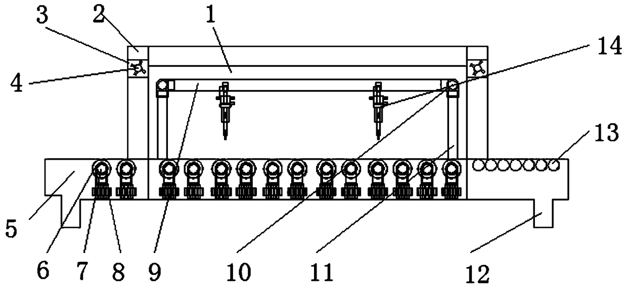
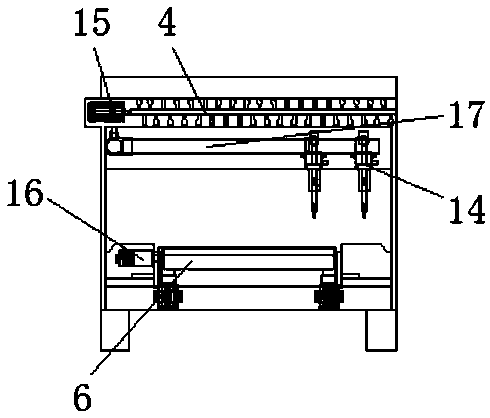
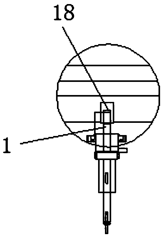
[0023] see Figure 1-3 , the present invention provides a technical solution: a PCB circuit board double-needle etching machine robot, including an etching chamber A01, a fixed rod A02, an air outlet chamber A03, a fan column A04, a storage table A05, a roller A06, and a first rotating shaft A07 , fixed base A08, first moving rod A09, connecting shaft A10, fixed frame A11, transmission leg A12, second rotating shaft A13, etching needle A14, first motor A15, se...


PUM


Abstract

The invention discloses a dual-needle etching robot of a PCB. The dual-needle etching robot comprises an etching chamber, air outlet chambers and a placement table, wherein fixed rods are connected with a left side and a right side of the etching chamber, the air outlet chambers are arranged above inner sides of the fixed rods, fan posts are fixedly arranged at middle ends of inner cavities of theair outlet chambers, the placement table is fixedly arranged at a bottom end of the etching chamber, rollers are arranged above the inner cavity of the placement table, a first rotation shaft is embedded to a middle end of each roller, a fixed base is connected to a lower end of the roller, fixed racks are arranged at a left end and a right end of an inner side of the etching chamber, connectionshafts are fixedly arranged at the tops of the fixed racks, a first moving rod is arranged at a middle end between the connection shafts, transmission legs are connected to a lower end of the placement table, and a second rotation shaft is embedded to a right end of an upper side of the etching chamber. In the dual-needle etching robot of the PCB, the rollers are arranged and are distributed alongan upper end of an inner wall of the placement table, the rollers are driven by a second motor, and the transmission effects of the rollers on the PCB can be achieved.

Description

technical field [0001] The invention relates to the technical field of etching machine devices, in particular to a PCB circuit board double-needle etching machine robot. Background technique [0002] PCB, the Chinese name is printed circuit board, referred to as printed board, is one of the important components of the electronics industry. Almost every kind of electronic equipment, ranging from electronic watches and calculators to computers, communication electronic equipment, and military weapon systems, as long as there are electronic components such as integrated circuits, printed boards are used for the electrical interconnection between them. . In the larger electronic product research process, the most basic success factors are the design, documentation and fabrication of the product's printed board. The design and manufacturing quality of printed boards directly affect the quality and cost of the entire product, and even lead to the success or failure of commercial...

Claims


Application Information

Patent Timeline
Patent Type & Authority Applications(China)
IPC IPC(8): H05K3/06
CPCH05K3/068H05K2203/081
Inventor 周立新
Owner 周立新
Why Eureka
Try Eureka