Low temperature polysilicon thin film transistor and manufacturing method thereof and display device

A low-temperature polysilicon and thin-film transistor technology, which is applied in the direction of transistors, semiconductor/solid-state device manufacturing, semiconductor devices, etc., can solve problems such as increasing production costs, and achieve the effects of overcoming production costs, simplifying production processes, and reducing production costs

Inactive Publication Date: 2018-12-07
WUHAN CHINA STAR OPTOELECTRONICS TECH CO LTD
View PDF4 Cites 1 Cited by
  • Summary
  • Abstract
  • Description
  • Claims
  • Application Information

AI Technical Summary

Problems solved by technology

[0005] The technical problem to be solved by the present invention is to provide a low-temperature polysilicon thin-film transistor and its manufacturing method, and a display device, so as to overcome the need for a separate design of a photomask for the patterning of the channel light-shielding layer of the traditional low-temperature polysilicon thin-film transistor. The disadvantage of production cost

Method used


Image

  • Low temperature polysilicon thin film transistor and manufacturing method thereof and display device
  • Low temperature polysilicon thin film transistor and manufacturing method thereof and display device
  • Low temperature polysilicon thin film transistor and manufacturing method thereof and display device

Examples


Embodiment Construction

[0047] The following descriptions of various embodiments refer to the accompanying drawings to illustrate specific embodiments in which the present invention can be implemented.

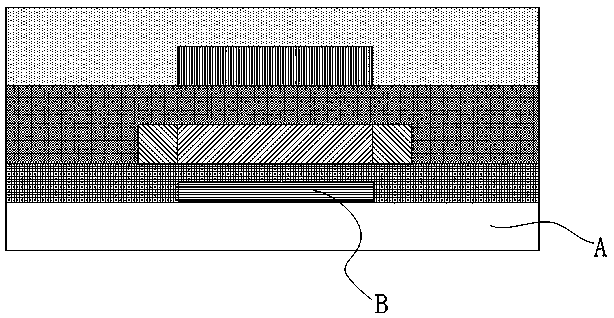
[0048] like figure 2 Shown is a method for manufacturing a low-temperature polysilicon thin film transistor provided by an embodiment of the present invention, and the method includes the following steps:

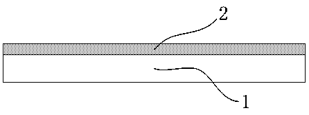
[0049] S100 providing a first substrate 1 and a second substrate 2;

[0050] In this embodiment, the first substrate 1 and the second substrate 2 are two substrates with the same thickness, length and width, both of which are made of glass, and the composition of the glass can be changed according to the actual situation, for example, The material of the glass is Na 2 SiO 3 , CaSiO 3 , SiO 2 ; Another example, the material of the glass is Na 2 O CaO 6SiO 2 For another example, polymethyl methacrylate can also be doped in the glass to obtain organic glass with strong chemical properties, so...


PUM


Abstract

The invention provides a low temperature polysilicon thin film transistor and a manufacturing method thereof and a display device. The low temperature polysilicon thin film transistor comprises a first substrate, a dielectric layer formed on the first substrate, a gate electrode layer formed on the dielectric layer, a gate electrode insulating layer formed on the gate electrode layer, a low temperature polysilicon layer and a doping layer which are formed on the gate electrode insulating layer and a buffer layer formed on the low temperature polysilicon layer. The manufacturing method is usedfor manufacturing the low temperature polysilicon thin film transistor. The display device comprises the low temperature polysilicon thin film transistor. The defects that when the conventional low temperature polysilicon thin film transistor is manufactured, a photomask needs to be separately designed for metal thin film patterning of the channel light shielding layer and the manufacturing cost is increased can be overcome.

Description

technical field [0001] The invention relates to the technical field of display device manufacturing, in particular to a low-temperature polysilicon thin film transistor, a manufacturing method thereof, and a display device. Background technique [0002] Low Temperature Poly-Si Thin Film Transistor (LTPS-TFT) has outstanding advantages such as high carrier mobility and small size, and is a key technology for the development of low-power, highly-integrated display panels. In order to suppress the photo-generated current of LTPS-TFT under light conditions and avoid the unintentional opening of thin film transistors (Thin Film Transistor, TFT), in the prior art, a layer of metal thin film is made before the production of low-temperature polysilicon thin film transistors. The metal thin film is patterned to form the channel light-shielding layer (LS, Light Shielding) of the low-temperature polysilicon thin film transistor. [0003] In the course of realizing the present inventio...

Claims


Application Information

Patent Timeline
Patent Type & Authority Applications(China)
IPC IPC(8): H01L29/06H01L21/336H01L29/786
CPCH01L29/0684H01L29/66742H01L29/786
Inventor 聂晓辉张嘉伟
Owner WUHAN CHINA STAR OPTOELECTRONICS TECH CO LTD
Why Eureka
Try Eureka