Mini LED backlight source, preparation method thereof and backlight source module

A backlight and module technology, applied in optics, nonlinear optics, instruments, etc., can solve problems such as poor screen contrast and non-local dimming, and achieve the goals of reducing power consumption, improving uniformity of light emission, and improving light source utilization Effect

Inactive Publication Date: 2018-12-11
SHANGHAI AVIC OPTOELECTRONICS
View PDF16 Cites 23 Cited by
  • Summary
  • Abstract
  • Description
  • Claims
  • Application Information

AI Technical Summary

Problems solved by technology

There are mainly two types of backlight module architectures: side-type and direct-type. The side-type LED backlight is to install the LED light source on the side of the light guide plate. Scattering directs light out, the disadvantage of this is that the contrast of the formed picture is relatively poor, and local dimming is not possible

Method used


Image

  • Mini LED backlight source, preparation method thereof and backlight source module
  • Mini LED backlight source, preparation method thereof and backlight source module
  • Mini LED backlight source, preparation method thereof and backlight source module

Examples


Embodiment Construction

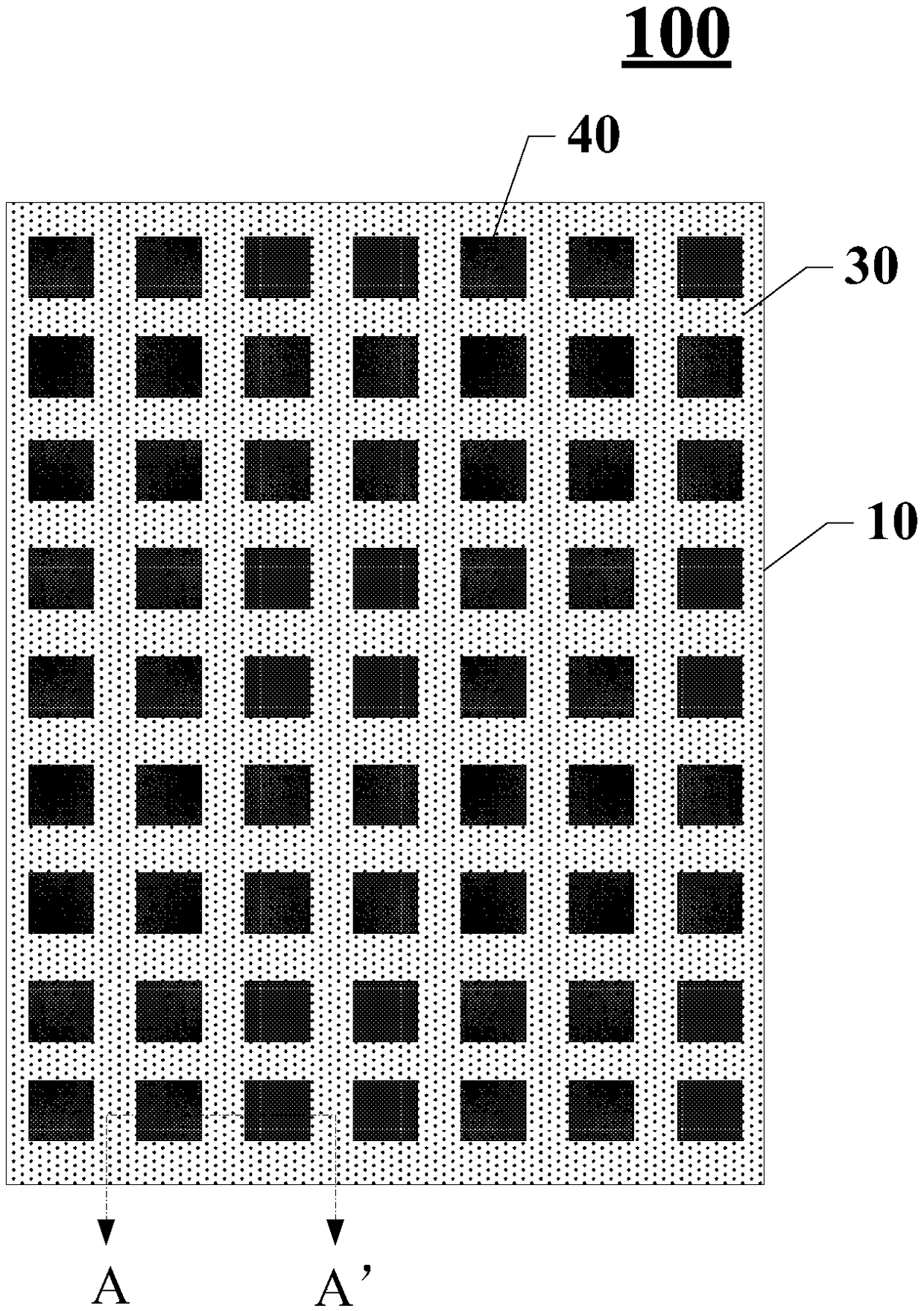
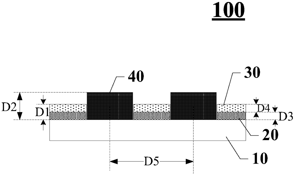
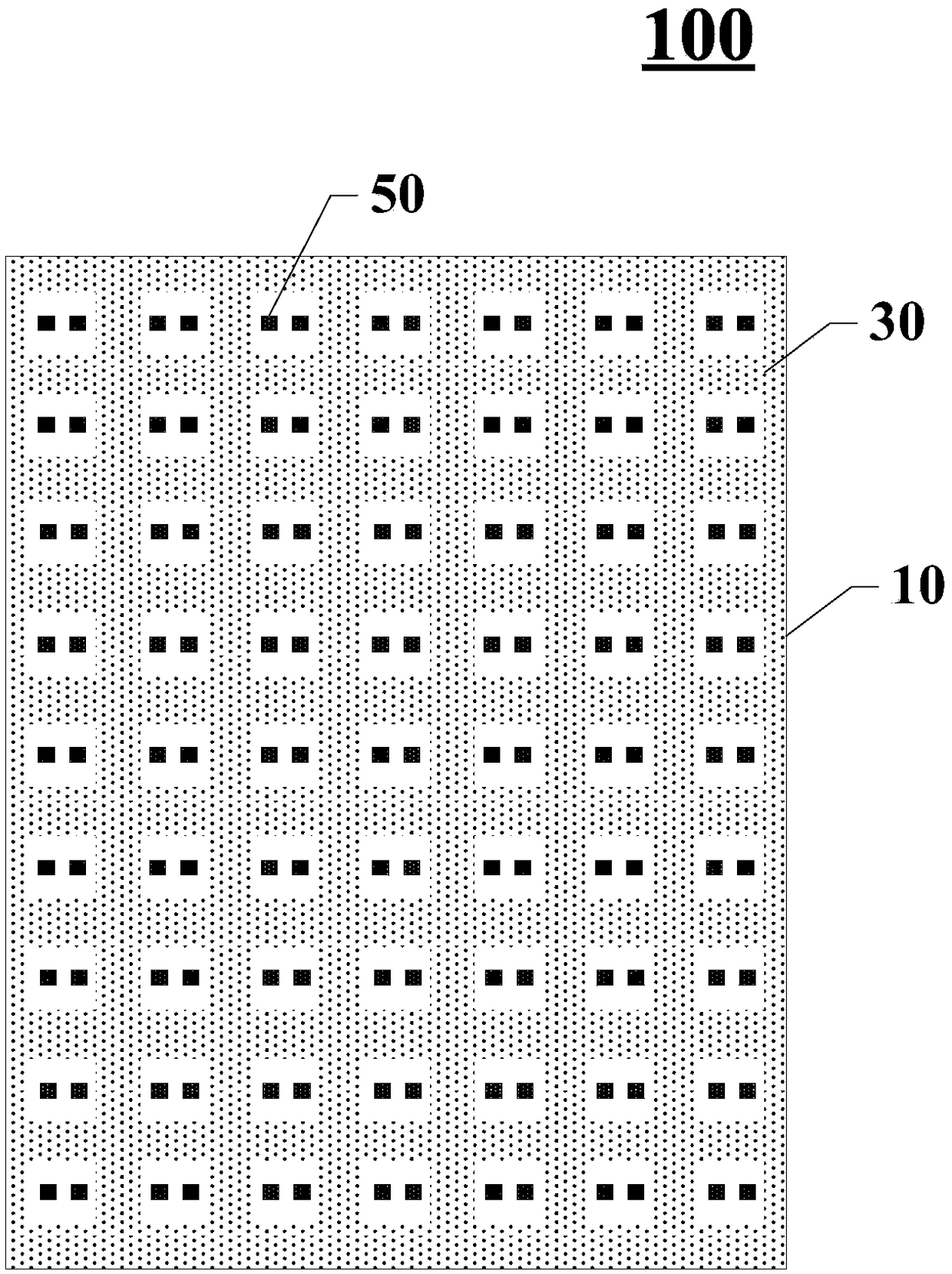
[0033] Various exemplary embodiments of the present invention will now be described in detail with reference to the accompanying drawings. It should be noted that the relative arrangement of components and steps, the numerical expressions and numerical values ​​set forth in these embodiments do not limit the scope of the invention unless specifically stated otherwise.

[0034] The following description of at least one exemplary embodiment is merely illustrative in nature and is in no way intended to limit the invention, its application, or uses.

[0035] Techniques, methods, and apparatus known to those of ordinary skill in the relevant art may not be discussed in detail, but where appropriate, such techniques, methods, and apparatus should be considered part of the specification.

[0036] In all examples shown and discussed herein, any specific values ​​should be construed as illustrative only and not limiting. Accordingly, other instances of the exemplary embodiment may hav...


PUM

PropertyMeasurementUnit
thicknessaaaaaaaaaa
thicknessaaaaaaaaaa
thicknessaaaaaaaaaa

Abstract

The invention discloses a mini LED backlight source, a preparation method thereof and a backlight source module, relating to the technical field of display. The mini LED backlight source comprises a substrate, a light reflection layer, a protection layer and multiple Mini LED chips. The substrate comprises multiple electrically-connected terminal pairs exposed on a first surface of the substrate.The light reflection layer is arranged on the first surface of the substrate. The reflection rate of the light reflection layer is n1 larger than or equal to 90%. The protection layer is arranged on the surface away from the substrate on the light reflection layer. The Mini LED chips are arranged on the first surface of the substrate and electrically connected with the electrically-connected terminals in the form of one-to-one correspondence. A light reflection layer is arranged between at least partially-adjacent Mini LED chips. The orthographic projection where the light reflection layer islocated on a plane of the substrate does not intersect with the Mini LED chips. The orthographic projection where the light reflection layer is located on the plane does not intersect with the Mini LED chips. The distance between the surface, away from the substrate, of the protection layer and the substrate is D1. The distance between the surface, away from the substrate, of the Mini LED chips and the substrate is D2. D1 is smaller than or equal to D2. Brightness of the backlight source is increased while power consumption is reduced.

Description

technical field [0001] The present invention relates to the field of display technology, and more particularly, to a Mini LED backlight source, a preparation method thereof, and a backlight source module. Background technique [0002] At present, the application penetration rate of LED as a backlight source in the field of liquid crystal panel display has exceeded 90%. There are two main types of backlight module architectures: side-light and direct-light. The side-light LED backlight is to set the LED light source on the side of the light guide plate, and the light emitted by the LED enters the light guide plate through coupling, and passes through the reflection sheet and the reflection of the dots. Scattering leads the light out. The disadvantage of this is that the contrast of the picture formed is relatively poor, and local dimming is not possible. Direct-type LED backlights have gradually become the mainstream trend in the market to present images more accurately and ...

Claims


Application Information

Patent Timeline
Patent Type & Authority Applications(China)
IPC IPC(8): G02F1/13357
CPCG02F1/133603G02F1/133605G02F1/133608
Inventor 苏世虎
Owner SHANGHAI AVIC OPTOELECTRONICS
Why Eureka
Try Eureka