Optical imaging lens assembly, image capturing unit and electronic device

An optical imaging and mirror group technology, applied in optics, optical components, instruments, etc., can solve problems such as inability to take into account large apertures, volume limitations, etc.

Active Publication Date: 2018-12-18
LARGAN PRECISION
View PDF5 Cites 7 Cited by
  • Summary
  • Abstract
  • Description
  • Claims
  • Application Information

AI Technical Summary

Problems solved by technology

However, the size of portable electronic devices is limited, so the camera modules mounted on them often cannot meet the needs of large apertures while maintaining a wide viewing angle.

Method used


Image

  • Optical imaging lens assembly, image capturing unit and electronic device
  • Optical imaging lens assembly, image capturing unit and electronic device
  • Optical imaging lens assembly, image capturing unit and electronic device

Examples


no. 1 example

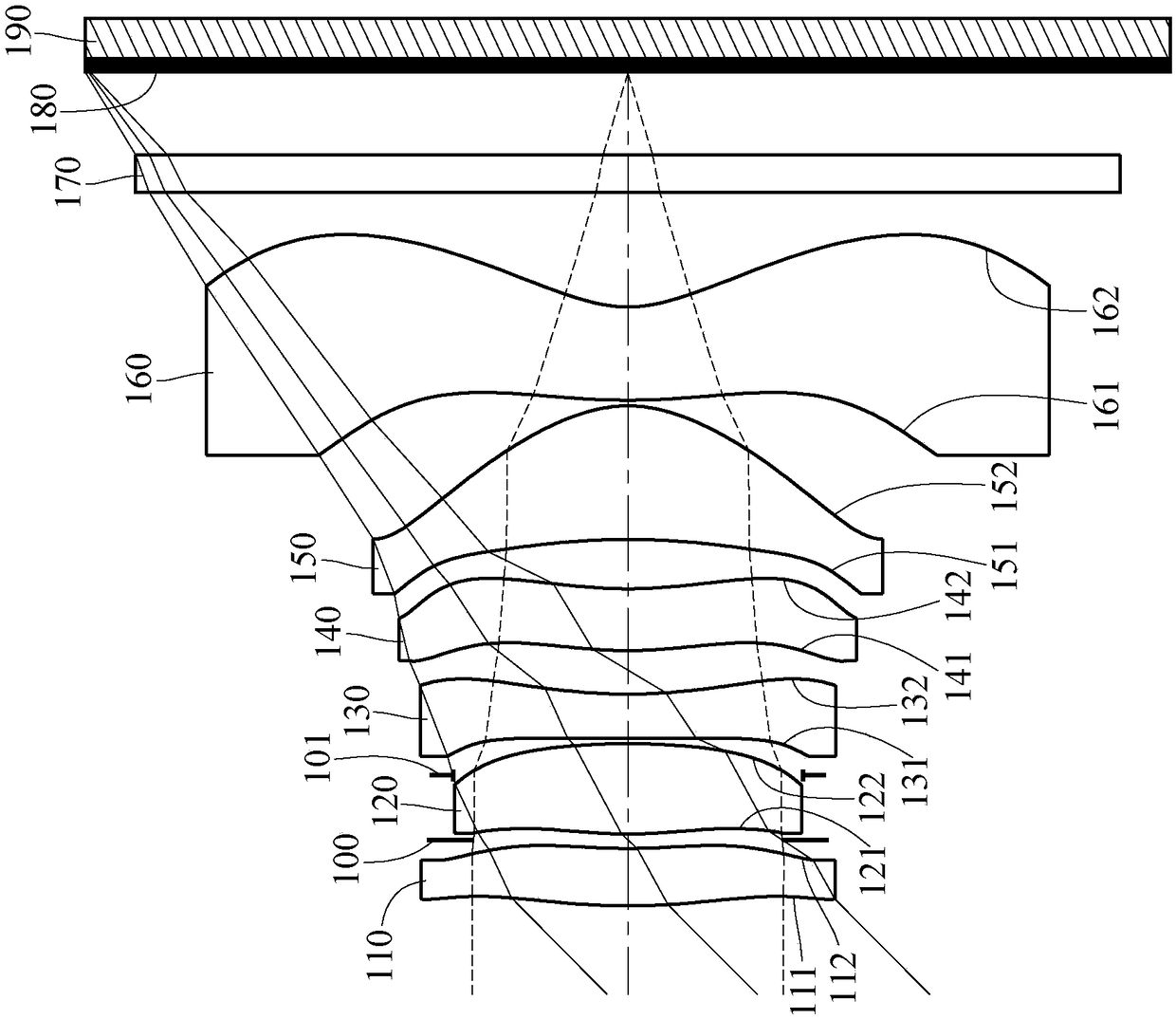
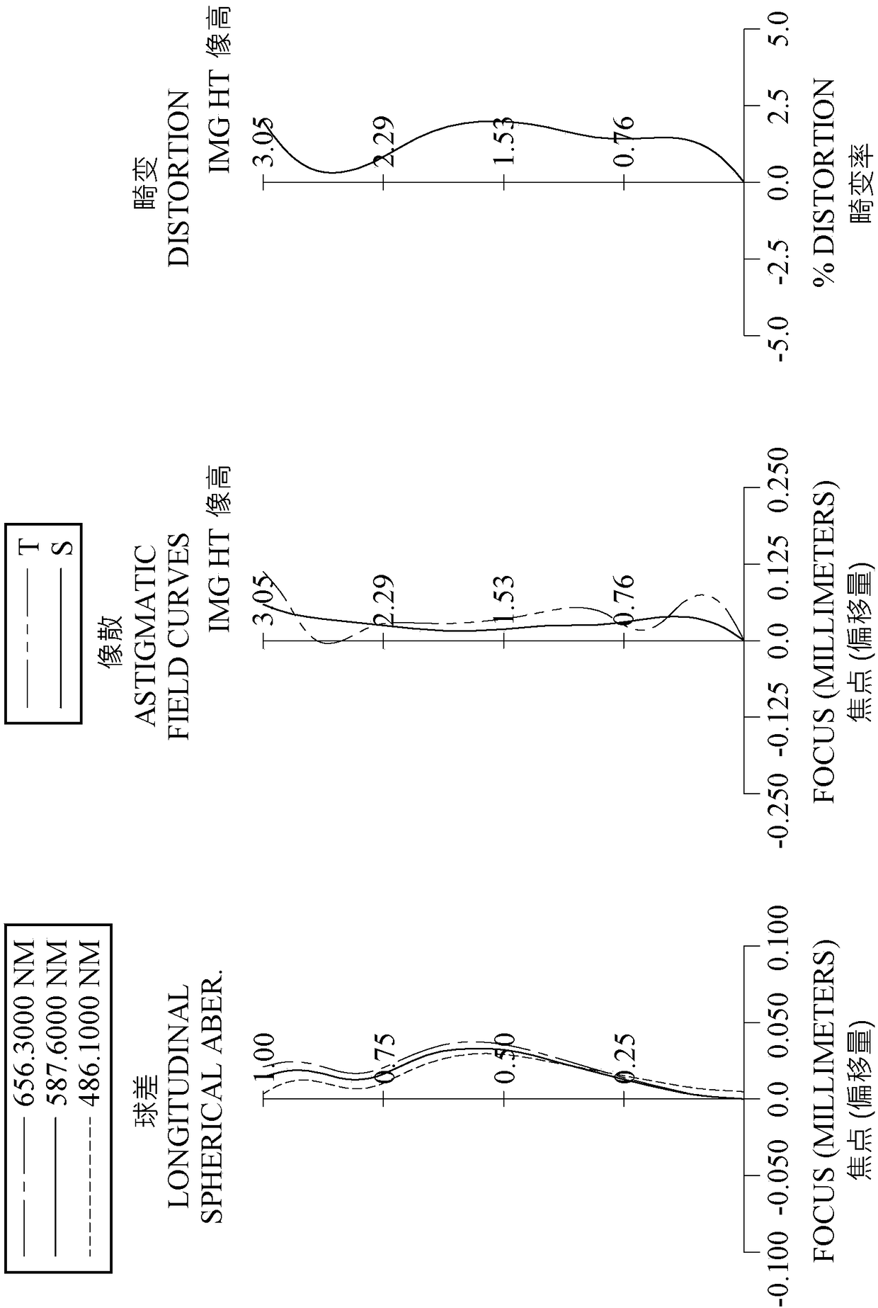
[0120] Please refer to Figure 1 to Figure 2 ,in figure 1 A schematic diagram of an imaging device according to a first embodiment of the present invention is shown, figure 2 From left to right are the spherical aberration, astigmatism and distortion curves of the first embodiment. Depend on figure 1 It can be seen that the image capturing device includes an optical image capturing mirror group (not another number) and an electronic photosensitive element 190 . The optical image capture lens group sequentially includes a first lens 110, an aperture 100, a second lens 120, an aperture 101, a third lens 130, a fourth lens 140, a fifth lens 150, and a sixth lens from the object side to the image side. 160 . An IR-cut filter element (IR-cut Filter) 170 and an imaging surface 180 . Wherein, the electronic photosensitive element 190 is disposed on the imaging surface 180 . The optical image capturing lens set includes six lenses ( 110 , 120 , 130 , 140 , 150 , 160 ), and there...

no. 2 example

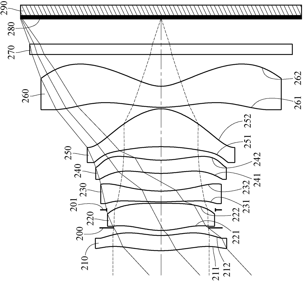
[0158] Please refer to Figure 3 to Figure 4 ,in image 3 A schematic diagram of an imaging device according to a second embodiment of the present invention is shown, Figure 4 From left to right are the spherical aberration, astigmatism and distortion curves of the second embodiment. Depend on image 3 It can be seen that the image capturing device includes an optical image capturing mirror group (not another number) and an electronic photosensitive element 290 . The optical image capture lens group includes a first lens 210, an aperture 200, a second lens 220, an aperture 201, a third lens 230, a fourth lens 240, a fifth lens 250, and a sixth lens in order from the object side to the image side. 260 . The infrared filter element 270 and the imaging surface 280 . Wherein, the electronic photosensitive element 290 is disposed on the imaging surface 280 . The optical image capturing mirror set includes six lenses ( 210 , 220 , 230 , 240 , 250 , 260 ), and there is no other...

no. 3 example

[0174] Please refer to Figure 5 to Figure 6 ,in Figure 5 A schematic diagram of an imaging device according to a third embodiment of the present invention is shown, Figure 6 From left to right are the spherical aberration, astigmatism and distortion curves of the third embodiment. Depend on Figure 5 It can be seen that the image capturing device includes an optical image capturing mirror group (not another number) and an electronic photosensitive element 390 . The optical image capture lens group includes a first lens 310, an aperture 300, a second lens 320, an aperture 301, a third lens 330, a fourth lens 340, a fifth lens 350, and a sixth lens in order from the object side to the image side 360 . The infrared filter element 370 and the imaging surface 380 . Wherein, the electronic photosensitive element 390 is disposed on the imaging surface 380 . The optical image capturing mirror set includes six lenses ( 310 , 320 , 330 , 340 , 350 , 360 ), and there is no other ...


PUM

PropertyMeasurementUnit
dispersion coefficientaaaaaaaaaa

Abstract

The invention discloses an optical imaging lens assembly. The optical imaging lens assembly includes, in order from an object side to an image side: a first lens element, a second lens element, a third lens element, a fourth lens element, a fifth lens element and a sixth lens element. The second lens element has positive refractive power. The third lens element has negative refractive power. The fifth lens element has positive refractive power. The sixth lens element has negative refractive power. At least one surface among object-side surfaces and image-side surfaces of the six lens elementsof the optical imaging lens assembly has at least one critical point in an off-axial region thereof and is aspheric.

Description

technical field [0001] The present invention relates to an optical image capturing mirror group, an image capturing device and an electronic device, in particular to an optical image capturing mirror group and an image capturing device suitable for an electronic device. Background technique [0002] In recent years, with the vigorous development of miniaturized photographic lenses, the demand for miniature photographic modules has increased day by day, and with the advancement of semiconductor technology, the pixel size of photosensitive elements has been reduced. The appearance of the development trend. Therefore, miniaturized photographic lenses with good imaging quality have become the mainstream in the current market. [0003] As the application of camera modules becomes more and more extensive, it will be a major trend of future technological development to install camera modules in various intelligent electronic products, vehicle devices, identification systems, enter...

Claims


Application Information

Patent Timeline
Patent Type & Authority Applications(China)
IPC IPC(8): G02B13/00G02B13/06G02B13/18
CPCG02B13/0045G02B13/06G02B13/18G02B1/007G02B1/04G02B13/001
Inventor 薛钧哲郭子杰
Owner LARGAN PRECISION
Why Eureka
Try Eureka