Film deposition apparatus

A deposition device and film layer technology, applied in electrical components, semiconductor/solid-state device manufacturing, circuits, etc., can solve problems such as unbalanced curvature distribution, and achieve the effect of improving quality and wide application

Pending Publication Date: 2018-12-18
YANGTZE MEMORY TECH CO LTD
View PDF8 Cites 7 Cited by
  • Summary
  • Abstract
  • Description
  • Claims
  • Application Information

AI Technical Summary

Problems solved by technology

[0006] The invention provides a film deposition device, which is used to solve the problem of unbalanced curvature

Method used


Image

  • Film deposition apparatus
  • Film deposition apparatus
  • Film deposition apparatus

Examples


Embodiment Construction

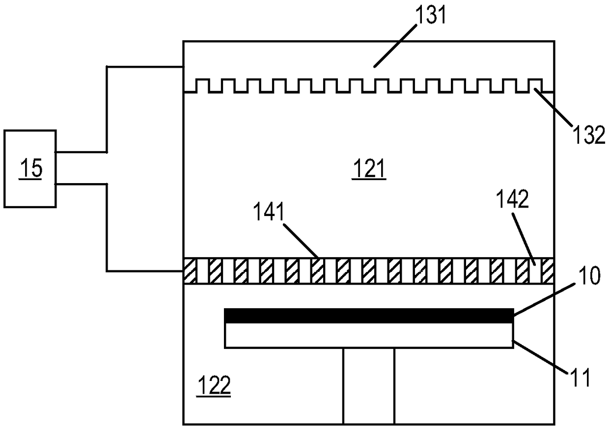
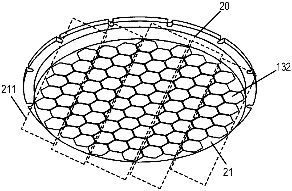
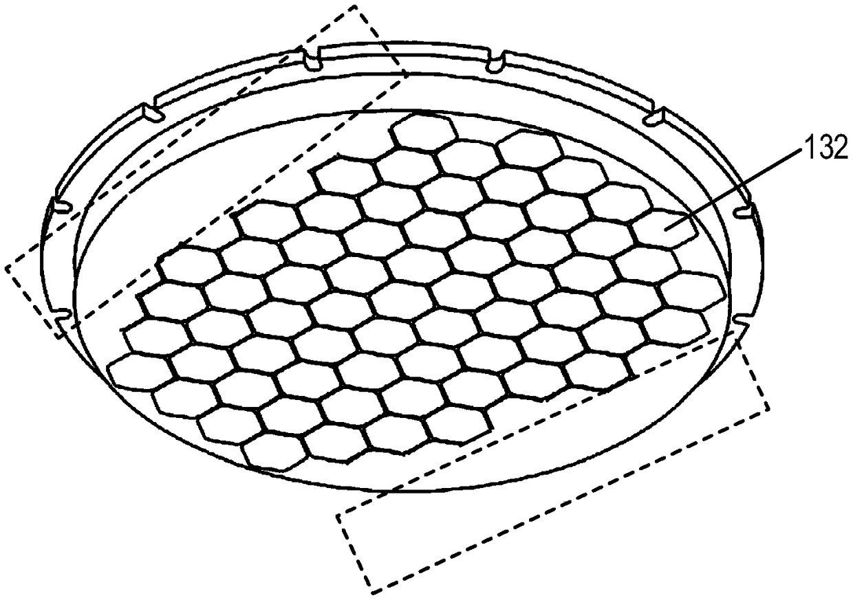
[0029] The specific implementation of the film deposition device provided by the present invention will be described in detail below with reference to the accompanying drawings.

[0030] During the manufacturing process of the wafer and the subsequent process of manufacturing electronic components on the surface of the wafer, the curvature distribution of the wafer may be unbalanced, resulting in warping of the wafer. The occurrence of wafer warpage will cause many problems, such as the peeling off of the laminated film on the wafer surface, wafer cracking, unstable layout alignment performance, and the sucker of the subsequent process cannot hold the wafer, etc., and the subsequent process cannot be completed, which will eventually lead to Instable performance of wafer products, and reduced yield and yield of wafer products.

[0031] Bowl-shaped wafers are a common unbalanced state of wafer bow distribution. For bowl-shaped wafers, the way to balance the curvature distributi...


PUM


Abstract

The invention relates to the technical field of semiconductor manufacturing, in particular to a film deposition device. The film deposition apparatus includes an adjusting portion including a partition surface disposed toward a wafer surface and a plurality of nozzles disposed on the partition surface for transferring reactants to the wafer surface; A control unit for controlling whether each of the nozzles is opened or not to realize the non-uniform distribution of the reactant density on the surface of the wafer. The invention can form a film layer with non-uniform thickness distribution onthe wafer surface, realizes the balance of wafer curvature distribution, is suitable for wafers with various shapes, and effectively improves the quality of wafer products.

Description

technical field [0001] The invention relates to the technical field of semiconductor manufacturing, in particular to a film deposition device. Background technique [0002] With the development of planar flash memory, the production process of semiconductors has made great progress. However, in recent years, the development of planar flash memory has encountered various challenges: physical limits, existing development technology limits, and storage electron density limits. In this context, in order to solve the difficulties encountered in planar flash memory and pursue lower production costs per unit storage unit, various three-dimensional (3D) flash memory structures have emerged, such as 3D NOR (3D or not) flash memory and 3D NAND (3D NAND) flash memory. [0003] Among them, 3D NAND memory takes its small size and large capacity as the starting point, and the design concept of highly integrated storage units stacked in three-dimensional mode is to produce a memory with ...

Claims


Application Information

Patent Timeline
IPC IPC(8): H01L21/67
CPCH01L21/67126H01L21/67288
Inventor 孟昭生徐文浩李展信刘聪
Owner YANGTZE MEMORY TECH CO LTD
Why Eureka
Try Eureka