A bidirectional false gate deep well electrostatic protection device for increasing failure voltage and a manufacturing method thereof

An electrostatic protection and device technology, applied in the field of bidirectional false gate deep well electrostatic protection devices, can solve problems such as insufficient protection capability, device latch-up effect, low maintenance voltage, etc., to avoid thermal breakdown, prevent latch-up effect, maintain Effects of current density and leakage current density reduction

Active Publication Date: 2018-12-18
SUPERESD MICROELECTRONICS TECH CO LTD
View PDF4 Cites 12 Cited by
  • Summary
  • Abstract
  • Description
  • Claims
  • Application Information

AI Technical Summary

Problems solved by technology

However, in the face of complex high-voltage environments, LDMOS-SCR still has insufficient protection capabilities. Under relatively large currents, it w

Method used


Image

  • A bidirectional false gate deep well electrostatic protection device for increasing failure voltage and a manufacturing method thereof
  • A bidirectional false gate deep well electrostatic protection device for increasing failure voltage and a manufacturing method thereof
  • A bidirectional false gate deep well electrostatic protection device for increasing failure voltage and a manufacturing method thereof

Examples


Embodiment Construction

[0033] The present invention will be further described below in conjunction with the accompanying drawings and embodiments.

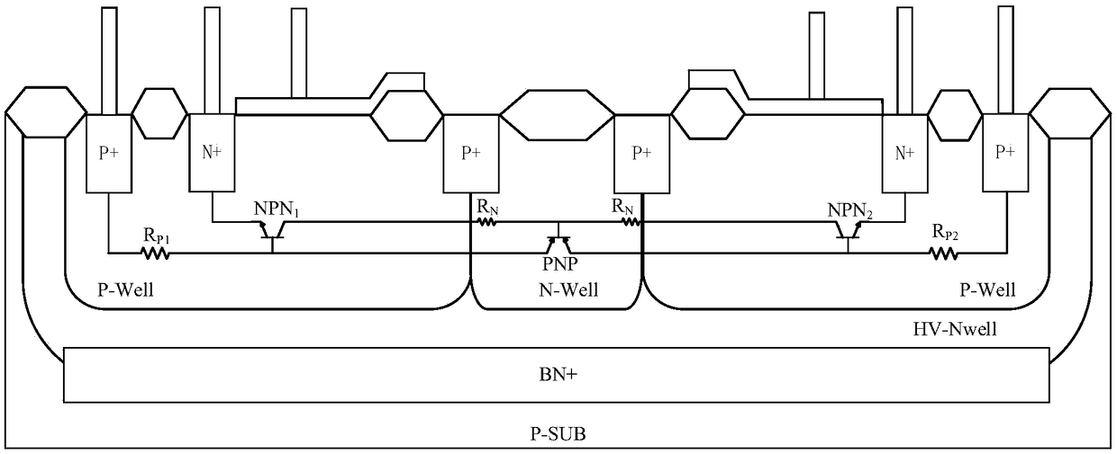
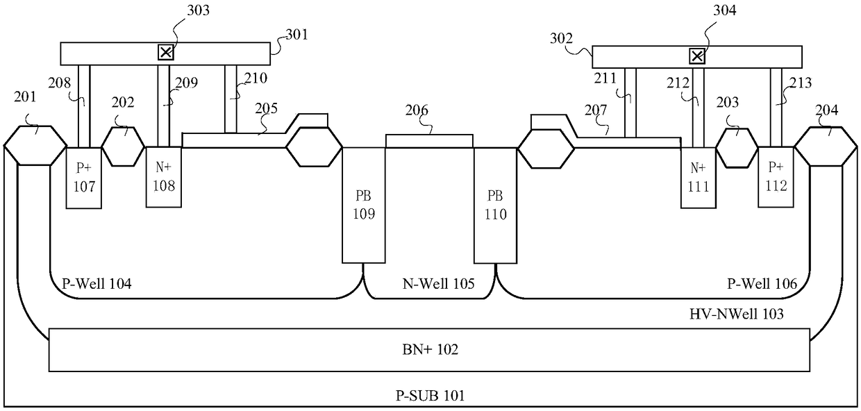
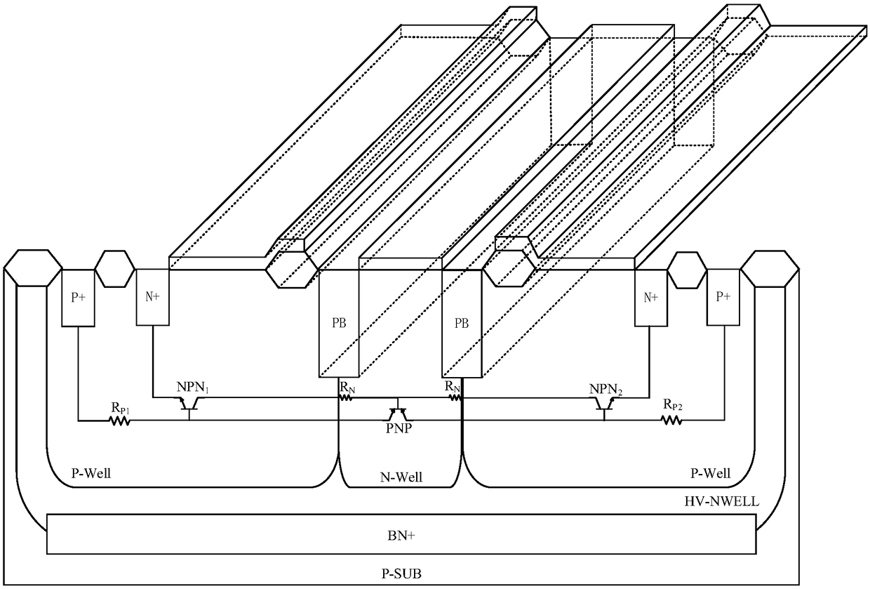
[0034] Such as Figure 2-Figure 4 As shown, a bidirectional dummy gate deep well electrostatic protection device with improved failure voltage includes a P-type substrate 101; an N-type buried layer 102 and a high-voltage N well 103 are arranged in the P-type substrate 101, and the high-voltage N well 103 is located above the N-type buried layer 102; the first P well 104, N well 105 and second P well 106 are arranged in the high-voltage N well 103 from left to right, and the left and right ends of the N well 105 are close to the first P well 104, second P well 106; the first P well 104 is provided with a first P+ implantation region 107 and a first N+ implantation region 108 from left to right; the first P well 104 and the N well 105 A first PB implantation region 109 is straddled between them; a second PB implantation region 110 is straddled between t...


PUM


Abstract

The invention discloses a bidirectional false gate deep well electrostatic protection device for increasing failure voltage, comprising a P-type substrate; an N-type buried layer and a high-voltage Nwell are arranged in the P-type substrate is provided with; a first P well, an N well and a second P well are arranged in the high-pressure N well; a first P+ implantation region and a first N+ implantation region are arranged in the first P well; a first PB implantation region is arranged between the first P well and the N well in a spanning manner; a second PB implantation region is arranged between the N well and the second P well in a spanning manner; the surface of the N well is provided with a first polysilicon dummy gate; a second N+ implantation region and a second P+ implantation region arranged in the second P well; and the first PB implantation region, the first polysilicon dummy gate, and the second PB implantation region constitute a polysilicon dummy gate deep well PB structure. The polysilicon dummy gate deep well PB structure of the invention can enable the ESD conduction path of the device to be bleeded in the N-type buried layer, the device can withstand high-intensity electrostatic pulse stress, and the device structure surface can be prevented from generating additional access, thereby effectively avoiding the phenomenon of thermal breakdown on the device surface.

Description

technical field [0001] The invention relates to the field of electrostatic protection, in particular to a bidirectional pseudo-gate deep well electrostatic protection device for increasing failure voltage and a manufacturing method thereof. Background technique [0002] With the passage of time, science and technology continue to advance, and the development of integrated circuits still follows the law of Moore's Law, that is, the miniaturization of device size and the increase of integration. The phenomenon of electrostatic discharge (ESD) is a major factor causing the failure of integrated circuits. Static electricity is everywhere and is closely related to people's lives. Therefore, more and more people begin to pay attention to the protection of ESD. According to relevant data, in the large In the background, the failure rate of electronic products due to ESD phenomenon is as high as 58%. This data fully shows that ESD protection is extremely important. An ESD protection...

Claims


Application Information

Patent Timeline
IPC IPC(8): H01L27/02
CPCH01L27/0262
Inventor 金湘亮汪洋
Owner SUPERESD MICROELECTRONICS TECH CO LTD
Why Eureka
Try Eureka