Eureka AIR delivers breakthrough ideas for toughest innovation challenges, trusted by R&D personnel around the world.

Array substrate, display panel and display device

An array substrate and backplane technology, applied in optics, instruments, electrical components, etc., can solve the problems of reduced pixel aperture ratio, large space occupation, and difficulty in adjusting the balance between the main area and the sub-area, so as to improve the alignment of liquid crystals. Effect

Active Publication Date: 2018-12-21
CHONGQING HKC OPTOELECTRONICS TECH CO LTD +1
View PDF10 Cites 2 Cited by
  • Summary
  • Abstract
  • Description
  • Claims
  • Application Information

AI Technical Summary

Problems solved by technology

Excessive TFT (Thin Film Transistor, thin film transistor) will lead to a decrease in the aperture ratio of the pixel itself, and due to the use of charge sharing technology, the pixel voltage between the main area and the sub area will be different, which will increase the pixel voltage between the main area and the sub area. The best common voltage (best V com ) the difficulty of balancing regulation
With the increase in the number of TFTs and the increase in multi-domains, the space is very large. In order to effectively use the design space, the line spacing will be reduced to a small size, resulting in an overlapping area between the supplementary electrode and the pixel electrode, which will have a shielding effect on the common electrode signal. Poor liquid crystal alignment is prone to occur

Method used


Image

  • Array substrate, display panel and display device
  • Array substrate, display panel and display device
  • Array substrate, display panel and display device

Examples


Embodiment approach

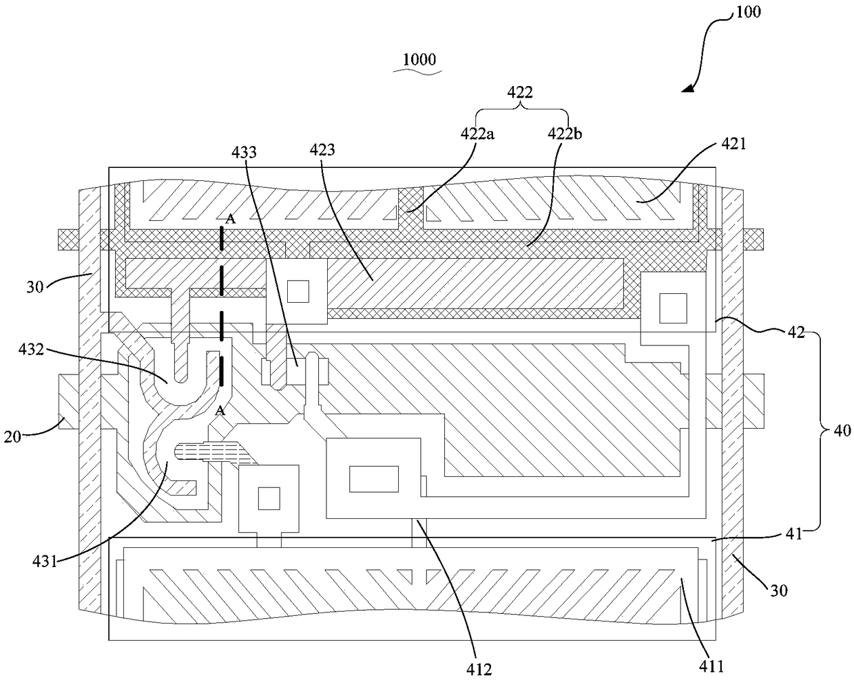
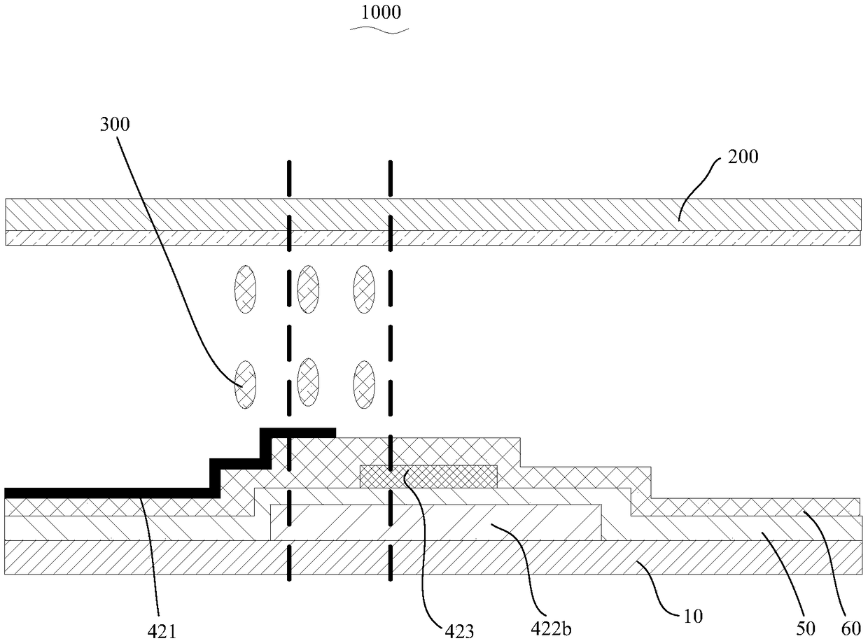
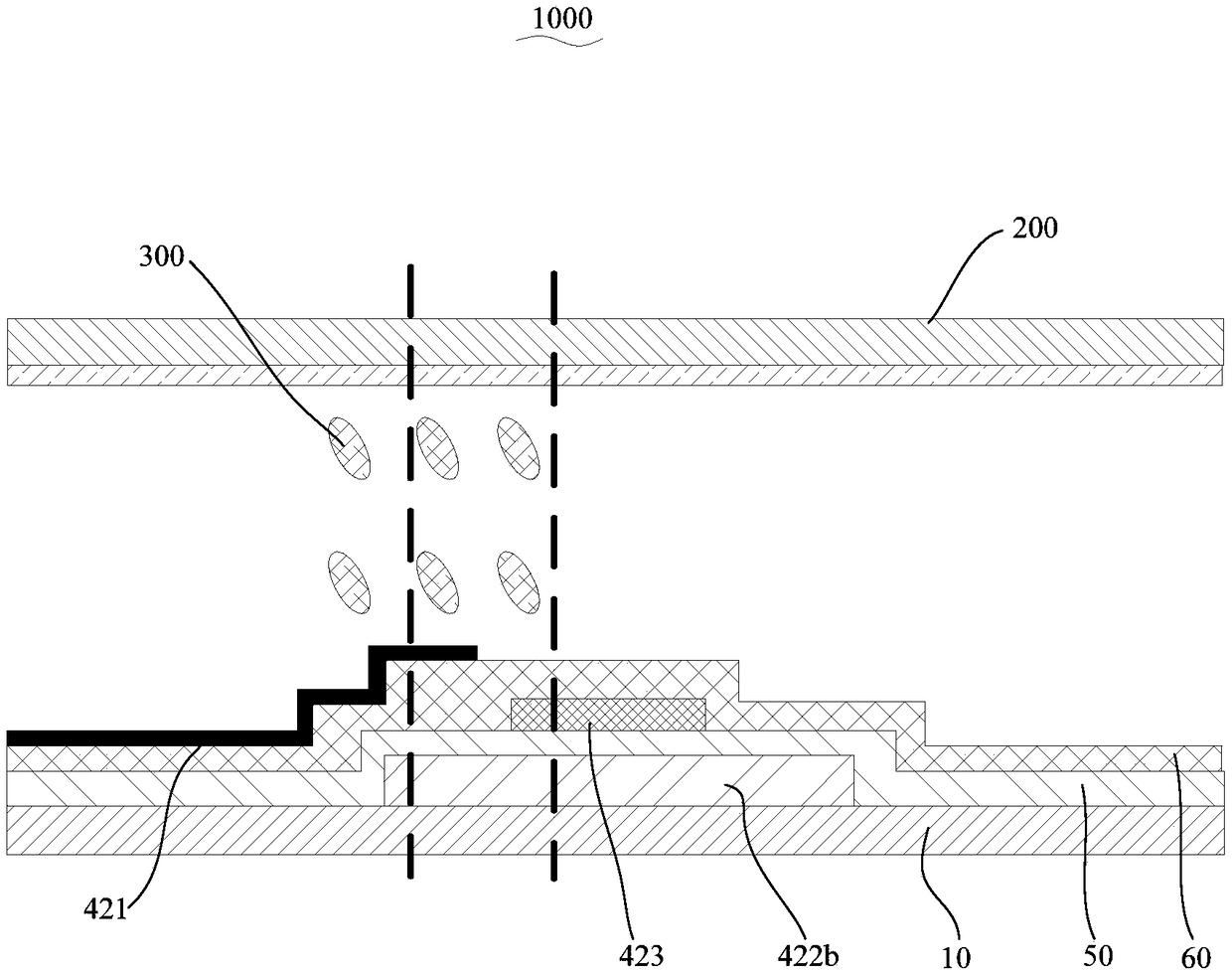
[0053] Specifically, since the projected area of ​​the compensation electrode 423 on the bottom plate 10 is not larger than the projected area of ​​the second common electrode 422b on the bottom plate 10, the storage capacitance of the pixel electrode 421 in the sub-region is reduced. In order to further reduce the V ft To balance the common voltage between the main region 41 and the sub-region 42 , it is necessary to increase the overlapping area between the pixel electrode 421 of the sub-region and the common electrode 422 of the sub-region. There are two implementation methods here. The first one is to increase the width of the first common electrode 422a along the extending direction of the scanning line 20, that is, to increase the distance between the light-shielding area of ​​the sub-region pixel electrode 421 and the first common electrode 422a. The overlapping area between them; the second one is to increase the width of the second common electrode 422b along the exten...


PUM


Abstract

The invention discloses an array substrate, a display panel and a display device. The array substrate comprises a bottom plate, wherein a subzone common electrode, a compensation electrode and a subzone pixel electrode are overlaid on the bottom plate in sequence; the compensation electrode and the subzone common electrode are in insulated arrangement, and the compensation electrode is electrically connected with the subzone pixel electrode through a through hole; the projection area of the compensation electrode on the bottom plate is not greater than the projection area of the subzone commonelectrode on the bottom plate; at least parts of the projection area of the subzone common electrode on the bottom plate are overlapped with the projection area of the subzone pixel electrode on thebottom plate; and the projection are of the compensation electrode on the bottom plate and the projection area of the subzone pixel electrode on the bottom plate are not mutually overlapped. Accordingto the array substrate, liquid crystal alignment ability can be improved.

Description

technical field [0001] The invention relates to the technical field of liquid crystal display, in particular to an array substrate, a display panel and a display device. Background technique [0002] In order to increase the viewing angle of liquid crystal displays, the existing technology usually adopts multi-domain technology, which divides a sub-pixel into multiple regions, and makes the liquid crystal in each region fall to different directions after voltage is applied. , so that the effects seen in all directions tend to be average and consistent. In order to improve visual chromatic aberration or visual color shift, in the prior art, a sub-pixel is divided into a main area and a sub-area, an independent main-area pixel electrode is set in the main area, and an independent sub-area pixel electrode is set in the sub-area, Both the pixel electrodes in the main area and the pixel electrodes in the sub area use rice-shaped slit electrodes to realize 8-domain display. Exce...

Claims


Application Information

Patent Timeline
Patent Type & Authority Applications(China)
IPC IPC(8): G02F1/1343G02F1/1362G02F1/139H01L27/12
CPCG02F1/134309G02F1/136227G02F1/136286G02F1/139G02F1/134318H01L27/124
Inventor 杨艳娜
Owner CHONGQING HKC OPTOELECTRONICS TECH CO LTD
Why Eureka
Eureka Blog
Learn More