Array substrate

A technology of array substrates and substrates, which is applied in the fields of instruments, computing, and electrical digital data processing, etc., and can solve problems such as increased production costs of array substrates and complicated production processes of array substrates.

Active Publication Date: 2020-10-16
WUHAN CHINA STAR OPTOELECTRONICS SEMICON DISPLAY TECH CO LTD
View PDF6 Cites 0 Cited by
  • Summary
  • Abstract
  • Description
  • Claims
  • Application Information

AI Technical Summary

Problems solved by technology

[0005] The present invention provides an array substrate to solve the problems that the production cost of the array substrate is increased and the production process of the array substrate is complicated due to the existence of insulating layers and touch wiring in the embedded touch display substrate

Method used


Image

  • Array substrate
  • Array substrate
  • Array substrate

Examples


Embodiment Construction

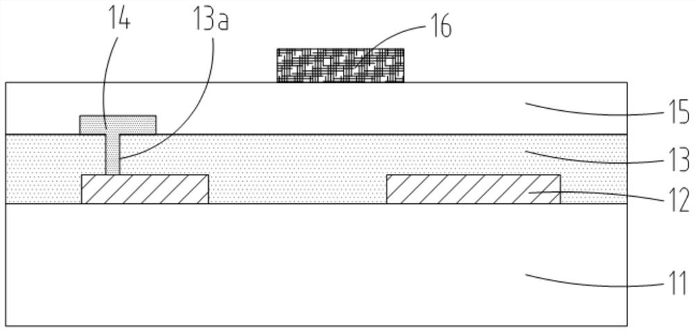
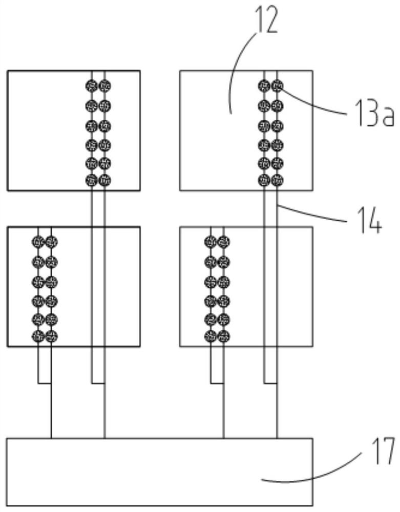
[0027] The following descriptions of the various embodiments refer to the accompanying drawings to illustrate specific embodiments in which the invention may be practiced. The directional terms mentioned in the present invention, such as [top], [bottom], [front], [back], [left], [right], [inside], [outside], [side], etc., are only for reference The orientation of the attached schema. Therefore, the directional terms used are used to illustrate and understand the present invention, but not to limit the present invention. In the figures, structurally similar elements are denoted by the same reference numerals.

[0028] The present invention provides an array substrate to solve the problems that the production cost of the array substrate is increased and the production process of the array substrate is complicated due to the existence of insulating layers and touch traces in the embedded touch display substrate. This embodiment can Improve this defect.

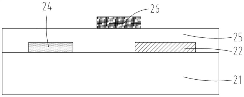
[0029] image 3 It is...


PUM


Abstract

An array substrate, comprising: a base substrate (21) and a touch electrode layer provided on the base substrate. The touch electrode layer comprises multiple touch electrodes (22) insulated from each other; the touch electrodes are electrically connected to a driving circuit (27) by means of touch wires (24); touch wires in adjacent touch electrodes are electrically connected by means of at least one bridge (26); the touch wires and the touch electrodes are disposed in the same layer, and the bridges and the touch electrodes are disposed in different layers.

Description

technical field [0001] The present invention relates to the display field, in particular to an array substrate. Background technique [0002] With the demand for thinner and lighter LCD panels, in-cell touch technology has become one of the necessary options for panels. Wherein, the structural difference between the in-cell touch display panel and the non-in-cell display panel is that the in-cell touch display panel has an additional layer structure: a touch wiring layer and an insulating layer. [0003] The structure of the embedded touch display substrate is as follows: figure 1 As shown, in the planar structure of the display area of ​​the in-cell touch display substrate, the touch electrodes are connected to the touch traces through insulating via holes. However, when designing the touch traces, only some of the touch traces are connected to the touch electrodes through insulating vias, and in order to simplify the embedded touch display substrate, the touch traces are...

Claims


Application Information

Patent Timeline
Patent Type & Authority Patents(China)
IPC IPC(8): G06F3/041G02F1/1333
CPCG02F1/13338G06F3/0412G06F3/0416
Inventor 赵瑜
Owner WUHAN CHINA STAR OPTOELECTRONICS SEMICON DISPLAY TECH CO LTD
Why Eureka
Try Eureka