A semiconductor device and a manufacturing method thereof

A manufacturing method and semiconductor technology, applied in the direction of semiconductor devices, electrical solid devices, electrical components, etc., can solve the problems of area waste, unfavorable device or circuit layout, etc.

Active Publication Date: 2018-12-21
南京市臻坤智能科技有限公司
View PDF6 Cites 1 Cited by
  • Summary
  • Abstract
  • Description
  • Claims
  • Application Information

AI Technical Summary

Problems solved by technology

However, since the current anti-static diodes have a planar structure, for some devices or circuits, if you want to increase the protection voltage of the diodes, you need to connect more diodes in series to achieve voltage division. This is an inevitable waste of area and is not conducive to the device. or circuit layout

Method used


Image

  • A semiconductor device and a manufacturing method thereof
  • A semiconductor device and a manufacturing method thereof
  • A semiconductor device and a manufacturing method thereof

Examples


Embodiment Construction

[0012] The technical solutions of the present invention will be further described in detail below in conjunction with the accompanying drawings and embodiments.

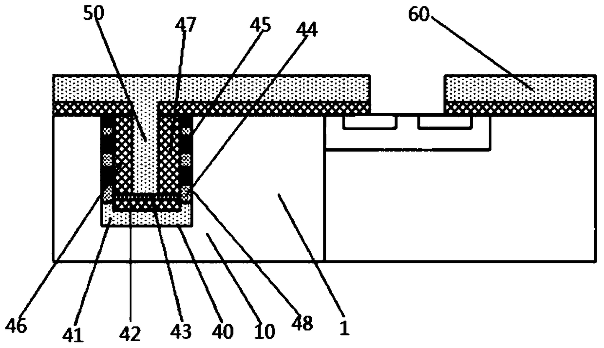
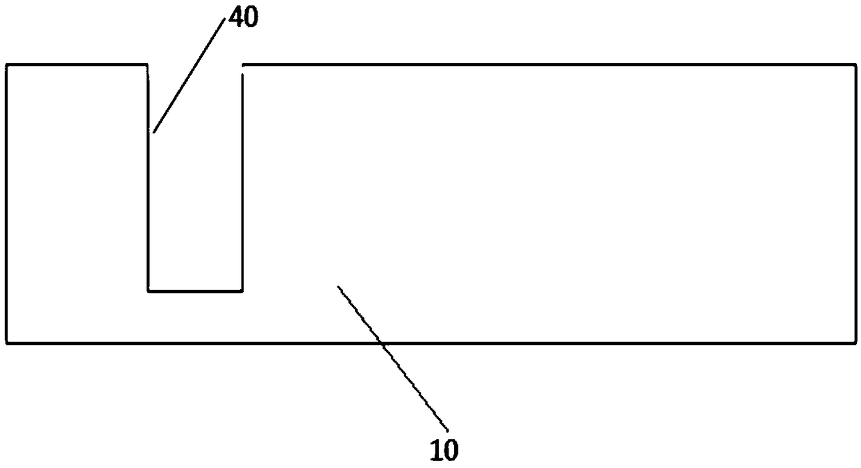
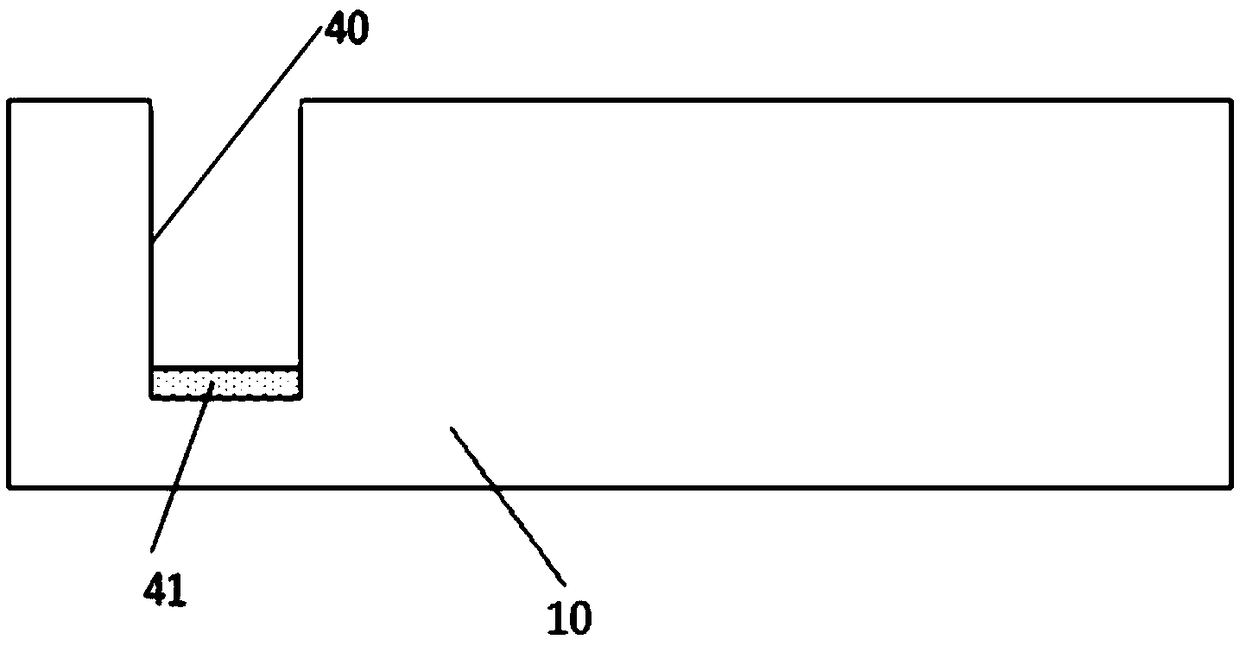
[0013] see figure 1 , the semiconductor device 1 includes a substrate 10, a trench 40 formed on the substrate 10, a compensation layer 41 of the first conductivity type formed at the bottom of the trench 40, a first oxide layer formed on the compensation layer 41 42. The wiring layer 43 formed on the first oxide layer 42, at least one first implantation region 44 of the second conductivity type and at least one second implantation region of the first conductivity type formed on the sidewall of the trench 40 region 45, the first electrode 50 and the second electrode 60, the first injection region 44 and the second injection region 45 are spaced apart, the top of the sidewall of the trench 40 is the second injection region 45, the The first electrode 50 is electrically connected to the first injection region 44 throug...


PUM


Abstract

A semiconductor device includes a substrate, a trench formed on the substrate, a compensation layer of a first conductivity type formed at the bottom of the trench, a first oxide layer formed on the compensation layer, a lead layer formed on the first oxide layer, at least one first injection region having a second conductivity type and at least one second injection region having a first conductivity type formed on the sidewall of the trench, a first electrode and a second electrode, wherein the first injection region is spaced apart from the second injection region, the top of the trench sidewall is a second injection region, the first electrode is electrically connected with the first injection region through the lead layer, and the second electrode is electrically connected with the compensation layer. The invention also provides a manufacturing method of a semiconductor device, which not only reduces waste of integrated area, enhances voltage withstand ability and reduces manufacturing cost, but also facilitates layout of the semiconductor device or circuit.

Description

technical field [0001] The invention belongs to the technical field of semiconductor device manufacturing technology, and in particular relates to a semiconductor device and a manufacturing method thereof. Background technique [0002] As semiconductor devices become increasingly smaller, denser, and more versatile, electronic devices are increasingly susceptible to electrostatic discharge (ESD) and other voltage surges that can even cause fatal injuries. Transient voltage suppressor (TVS) is a kind of device used to protect sensitive semiconductor devices. It has the advantages of small clamping coefficient, small size, fast response, small leakage current and high reliability. Due to various voltages from electrostatic discharge to lightning Surges can induce transient current spikes, and transient voltage suppressors (TVS) are often used to protect sensitive circuits from surges. [0003] Based on different applications, the transient voltage suppressor can protect the c...

Claims


Application Information

Patent Timeline
Patent Type & Authority Applications(China)
IPC IPC(8): H01L27/02H01L29/06
CPCH01L27/0255H01L29/0603H01L29/0615
Inventor 不公告发明人
Owner 南京市臻坤智能科技有限公司
Why Eureka
Try Eureka