A PFC inductance and battery boost transformer integrated topology
A technology of battery boosting and topology structure, which is applied in the direction of adjusting electrical variables, high-efficiency power electronic conversion, instruments, etc., and can solve the problems of many components and complicated circuits.
- Summary
- Abstract
- Description
- Claims
- Application Information
AI Technical Summary
Problems solved by technology
Method used
Image

Examples
Embodiment Construction
[0021] The technical solutions of the present invention will be further described below in conjunction with the accompanying drawings and through specific embodiments.
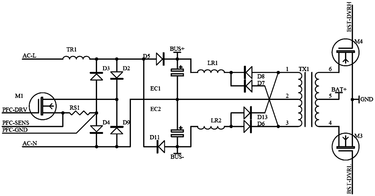
[0022] An integrated topology structure of a PFC inductor and a battery boost transformer, including a voltage stabilizing module and a power supply boost module;
[0023] The voltage stabilizing module works in the commercial power mode, and the voltage stabilizing module provides stable positive and negative BUS voltages and corrects power factor;
[0024] The power supply boost module turns to the battery-powered working state when the mains power is abnormal, and boosts the battery voltage into a stable positive and negative BUS.
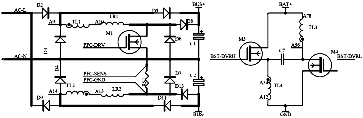
[0025] Such as figure 1 and figure 2 As shown, the topological structure of the present invention is the front-end circuit unit of the online UPS, which aims to provide stable positive and negative BUS power for the following inverter unit (the circuit that converts direct cu...
PUM
 Abstract
Description
Claims
Application Information
 - Generate Ideas
- Intellectual Property
- Life Sciences
- Materials
- Tech Scout
- Unparalleled Data Quality
- Higher Quality Content
- 60% Fewer Hallucinations
Browse by: Latest US Patents, China's latest patents, Technical Efficacy Thesaurus, Application Domain, Technology Topic, Popular Technical Reports.
© 2025 PatSnap. All rights reserved.Legal|Privacy policy|Modern Slavery Act Transparency Statement|Sitemap|About US| Contact US: help@patsnap.com