Correction method for self-aligned dual patterning process and semiconductor device thereof

A double patterning and self-alignment technology, applied in semiconductor/solid-state device manufacturing, electrical components, circuits, etc., can solve problems such as uneven key dimensions, tilted morphology, and poor etched film structure morphology, achieving Consistent critical dimension uniformity and improved morphology, the effect of improving critical dimensions and morphology

Active Publication Date: 2018-12-28
SHANGHAI HUAHONG GRACE SEMICON MFG CORP
View PDF6 Cites 5 Cited by
  • Summary
  • Abstract
  • Description
  • Claims
  • Application Information

AI Technical Summary

Problems solved by technology

The loading effect during core layer etching worsens the irregular morphology of the edge core pattern structure
The contact surface between the edge isolation structure and the edge core layer pattern is an inclined surface matching the trapezoidal surface of the core layer pattern, rather than a vertical surface, and the width of the edge isolation structure increases, then the etching film is etched on the basis of the isolation structure. The critical dimension (Critical Dimension, CD) of the edge etched film structure in the etched film structure formed after etching presents a defect that is not uniform with the critical dimensions of other etched film structures, and the morphology is inclined, that is, the edge etched film structure The critical dimension of the film structure is larger than that of other etched film structures, and the morphology of the etched film structure is not good

Method used


Image

  • Correction method for self-aligned dual patterning process and semiconductor device thereof
  • Correction method for self-aligned dual patterning process and semiconductor device thereof
  • Correction method for self-aligned dual patterning process and semiconductor device thereof

Examples


Embodiment Construction

[0025] The present invention is described in detail below in conjunction with accompanying drawing:

[0026] Please refer to Figure 14 , an embodiment of the present invention provides a method for correcting a self-aligned double patterning process, comprising the following steps:

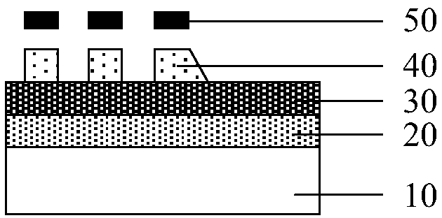
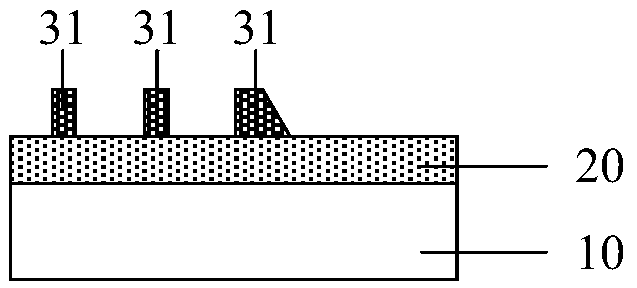
[0027] Step 901, please refer to Figure 7 , providing a substrate 100 .

[0028] Step 902, please refer to Figure 7 , forming an etching film layer 110 on the substrate 100 .

[0029] Step 903, please refer to Figure 7 , forming a core layer 120 on the etched film layer 110 . The material of the core layer is, for example, oxides such as silicon dioxide.

[0030] Step 904, please refer to Figure 7 , coating a photoresist layer 130 on the core layer 120 .

[0031] Step 905, please refer to Figure 7, set a core layer mask (core mask) 140, and add a group of mask structures 141 with the same specification next to the position of the core layer mask 140 corresponding to the core pattern...


PUM


Abstract

The invention provides a correction method for a self-aligned dual patterning process and semiconductor device thereof. The method comprises: forming an etching film layer, a core layer and a photoresist layer on a substrate. The photoresist layer is photolithographically etched after the core layer mask is added with a mask structure to form a patterned photoresist structure; the core layer is etched on the basis of the patterned photoresist structure to form the core pattern structure. Spacers are deposited on the core pattern structure and etched to form spacer layers on both sides of the core pattern structure; the core graphics structure are removed and the spacer layer is kept; a photoresist is applied on the spacer layer; on the peripheral mask, after the position of the peripheraletching film structure to be etched and the edge spacer layer with irregular shape are formed and covered, the photoresist is photolithographically etched to form the peripheral photoresist structure;a modified etched film structure is formed by etching the etched film layer with a spacer layer and a peripheral photoresist structure as a mask. The invention can improve the uniformity and the morphology of the key dimensions of the etched film.

Description

technical field [0001] The invention relates to the technical field of semiconductor manufacturing, in particular to a method for correcting a self-aligned double patterning process and a semiconductor device thereof. Background technique [0002] Self-aligned double patterning (Self Aligned Double Patterning, SADP) technology has been widely used in semiconductor manufacturing process. Please refer to Figure 1 to Figure 6 , the traditional self-aligned double patterning process is as follows: a substrate 10 is provided, an etching film layer 20 and a core layer 30 are sequentially formed on the substrate 10, and a photoresist is coated on the core layer 30 and formed through a mask plate 50 The photoresist pattern 40, based on the photoresist pattern 40, the core layer 30 is etched to form a core pattern structure 31, and the spacers are deposited to form a self-aligned spacer layer 60 on both sides of the core pattern structure 31, and the spacer layer 60 Including the l...

Claims


Application Information

Patent Timeline
Patent Type & Authority Applications(China)
IPC IPC(8): H01L21/027H01L21/033
CPCH01L21/0274H01L21/0332H01L21/0337H01L21/0338
Inventor 叶滋婧
Owner SHANGHAI HUAHONG GRACE SEMICON MFG CORP
Why Eureka
Try Eureka