Supercharge Your Innovation With Domain-Expert AI Agents!

Chip comprehensive detection device

A kind of testing equipment and comprehensive technology, applied in the direction of semiconductor/solid-state device testing/measurement, electrical components, circuits, etc., can solve problems such as missed detection, troublesome operation, errors, etc., and achieve simple and convenient operation, improved efficiency, and high detection quality Guaranteed effect

Active Publication Date: 2019-01-01
泸州龙芯微科技有限公司
View PDF12 Cites 0 Cited by
  • Summary
  • Abstract
  • Description
  • Claims
  • Application Information

AI Technical Summary

Problems solved by technology

[0004] However, during the inspection process of the wafer, it is necessary to manually move the wafer continuously, and the operation is cumbersome
Moreover, there will always be errors through manual movement, which may easily lead to missed inspections in some places
At present, in order to realize the comprehensive inspection of the wafer, there is no device to realize the automatic movement of the wafer.

Method used


Image

  • Chip comprehensive detection device
  • Chip comprehensive detection device
  • Chip comprehensive detection device

Examples


Embodiment Construction

[0019] The following is further described in detail through specific implementation methods:

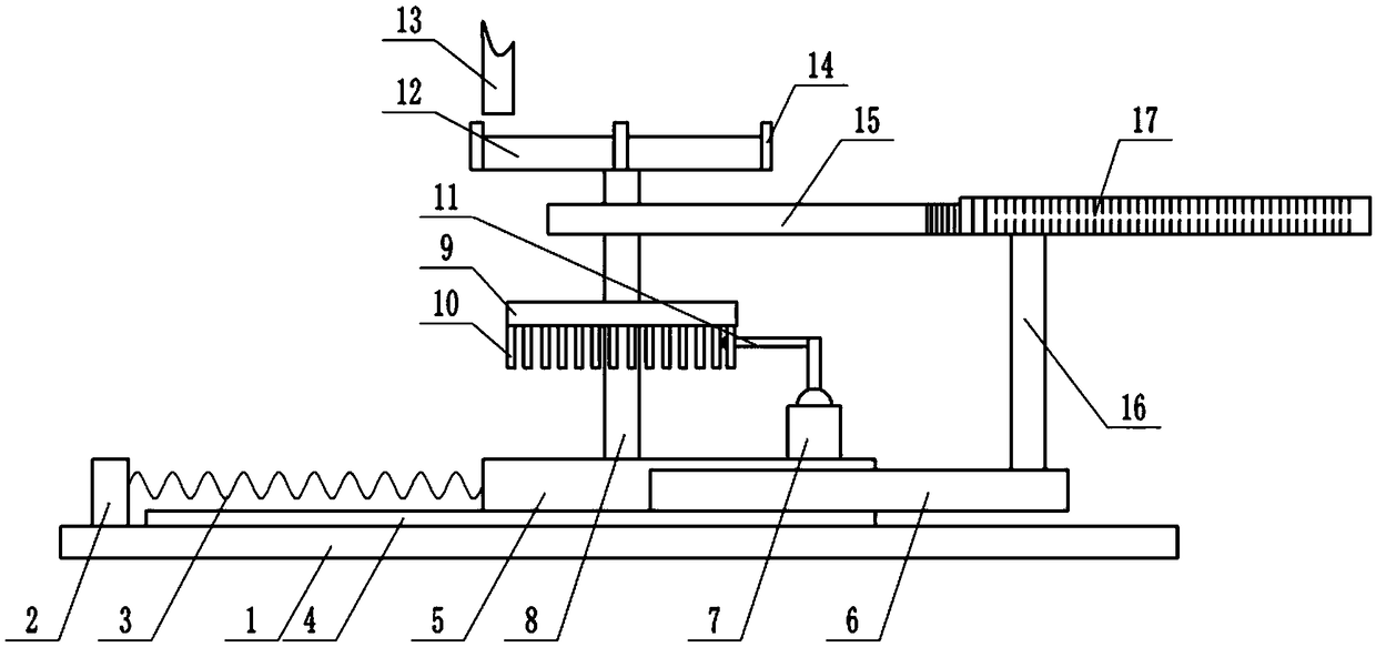
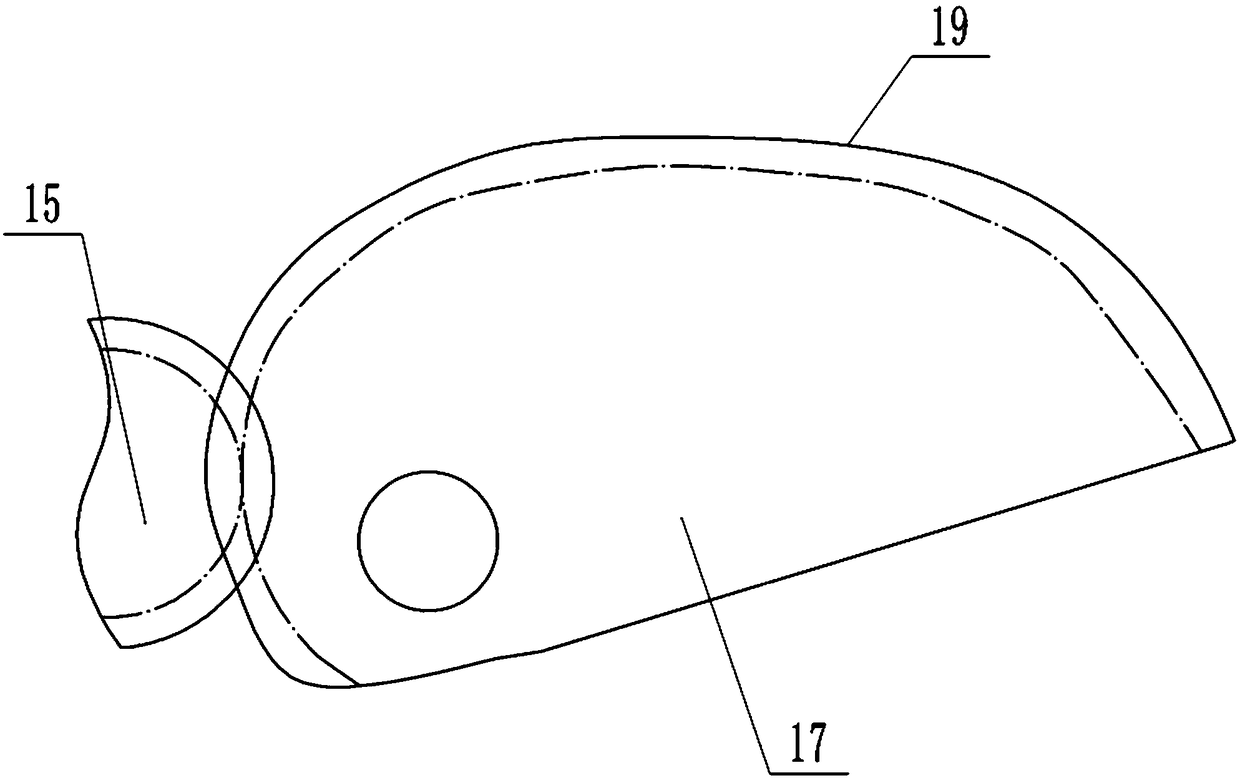
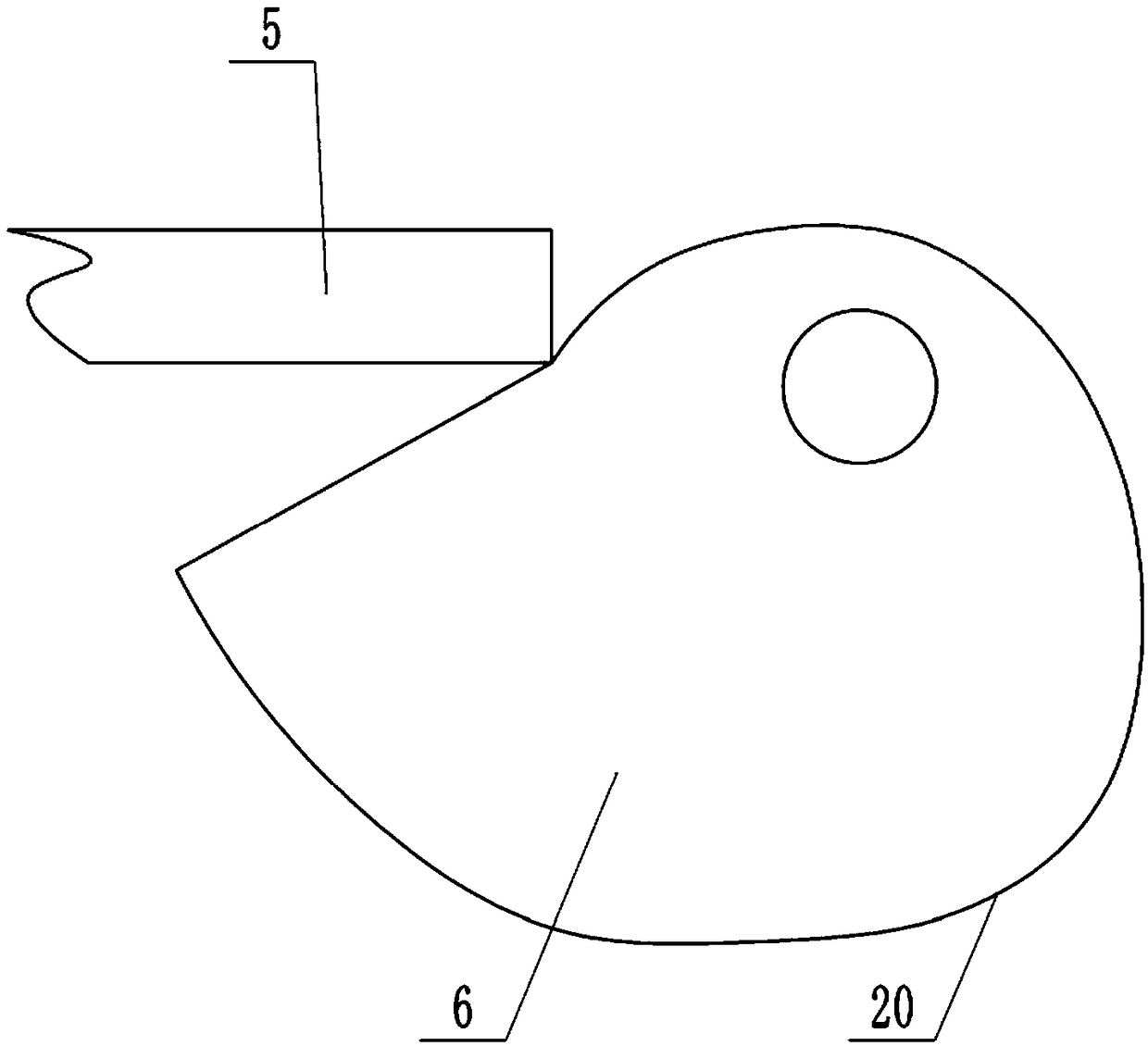
[0020] The reference signs in the accompanying drawings of the description include: fixed table 1, fixed block 2, compression spring 3, convex strip 4, sliding seat 5, cam 6, motor 7, rotating shaft 8, rotating disc 9, first driving lever 10, second Two driving rods 11, carrying platform 12, objective lens 13, limit block 14, first sector gear 15, connecting shaft 16, second sector gear 17, first circular path 18, tooth part 19, offset part 20, second annular Path 21.

[0021] The embodiment is basically as attached Figure 1-Figure 5 Shown: chip comprehensive inspection equipment, including frame, is provided with fixed platform 1 on the frame, is provided with microscope (not shown in the figure) and is positioned at the circular bearing platform 12 below the objective lens 13 of microscope above fixed platform 1 The carrier table 12 is used to place the wafer, and the carrier ta...


PUM


Abstract

The present invention relates to the field of chip detection, especially to a chip comprehensive detection device. The device comprises a microscope and a bearing platform located at the lower portionof the microscope, an objective lens of the microscope is opposite to the bearing platform, the bearing platform is connected with a rotation mechanism configured to rotate the bearing platform, andthe bearing platform is connected with a movement mechanism configured to perform horizontal movement of the bearing platform at intervals. The chip comprehensive detection device achieves automatic movement of the wafer and performs chip comprehensive detection.

Description

technical field [0001] The invention relates to the field of chip detection, in particular to chip comprehensive detection equipment. Background technique [0002] Wafer refers to the silicon wafer used in the production of silicon semiconductor integrated circuits. Because of its circular shape, it is called a wafer. During the processing of the wafer, the surface of the wafer needs to be polished, cut and cleaned. In order to detect the quality of wafer surface grinding, cutting and cleaning, and avoid defects or stains on the processed surface of the wafer, the processed wafer is often observed under a microscope to detect the processed surface of the wafer. [0003] Due to the relatively large diameter of the wafer, in order to be able to inspect the processing surface of the wafer in all directions, it is necessary to manually move the wafer, so that the objective lens of the microscope is opposite to each part of the processing surface of the wafer, so as to realize t...

Claims


Application Information

Patent Timeline
Patent Type & Authority Applications(China)
IPC IPC(8): H01L21/66
CPCH01L22/10H01L22/12H01L22/30
Inventor 颜文
Owner 泸州龙芯微科技有限公司
Features
  • R&D
  • Intellectual Property
  • Life Sciences
  • Materials
  • Tech Scout
  • Unparalleled Data Quality
  • Higher Quality Content
  • 60% Fewer Hallucinations
Learn More