
Laser encapsulation structure and method

A technology of laser encapsulation and mask plate, which is applied in the direction of laser welding equipment, manufacturing tools, welding equipment, etc., can solve the problems of affecting production efficiency, increasing load, and decreasing encapsulation accuracy, so as to simplify equipment complexity, reduce encapsulation error, The effect of improving packaging yield

Active Publication Date: 2020-09-11
SHANGHAI MICRO ELECTRONICS EQUIP (GRP) CO LTD
View PDF5 Cites 0 Cited by
  • Summary
  • Abstract
  • Description
  • Claims
  • Application Information

AI Technical Summary

Problems solved by technology

However, these two methods have a lot of problems under the condition of high-generation narrow borders: firstly, the size of the mask under the high-generation is relatively large, and the method of adsorption from above the mask becomes impossible due to the heavy mask; In the scheme of supporting the mask below, in order to prevent the chrome surface of the mask from scratching, it needs to face up, which will increase the distance between the mask and the package surface, and put forward greater requirements on the telecentricity of the galvanometer optical path.
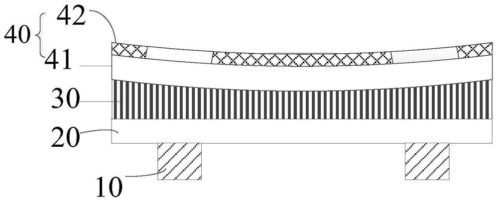
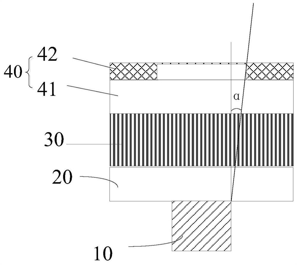
More importantly, there is a large gap between the mask surface and the substrate surface due to the support mechanism of the large-area mask, such as figure 1 As shown, the mask will be sunken due to its own weight, which will introduce a large unpredictable error, and finally lead to a decrease in packaging accuracy and seriously affect the packaging quality; figure 2 As shown, from bottom to top, the existing packaging structure includes the package lower substrate (not shown), the chip to be packaged with glass frit 10 around it, the package upper substrate 20, the gap layer 30, and the mask plate 40. The mask plate 40 includes glass The substrate 41 and the chrome surface 42 plated on the surface of the glass substrate 41, the gap layer 30 generated by the mask plate 40 and the packaging unit, and the thickness of the glass substrate 41 make higher requirements on the telecentric angle α of the optical path during the packaging process.
[0004] In addition, in the design of high-generation substrate packaging equipment, it is necessary to use a gantry to provide support for the movement of the substrate stage and the mask stage. The gantry has a large span and a large load. Therefore, the gantry cannot guarantee the movement accuracy and can only pass through the substrate stage. The movement is carried out, so that the mask stage also needs to move synchronously with the substrate stage during the packaging process, and a large alignment error will be introduced here
In addition, it is necessary to design a set of supporting, aligning, and moving components for the mask, which not only complicates the design of packaging equipment, but also inevitably adds the upper plate of the mask, the Accurate, remove these mask plate process, seriously affected the production efficiency

Method used


Image

  • Laser encapsulation structure and method
  • Laser encapsulation structure and method
  • Laser encapsulation structure and method

Examples


Embodiment 1

[0050] Please refer to Image 6 , the present invention provides a laser packaging method, comprising

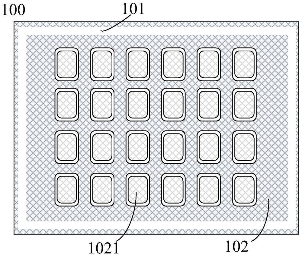
[0051] Step 1: Please refer to image 3 , set the mask to 100, specifically:

[0052] The mask 100 includes a glass substrate 104 and a chromium surface 102 sputtered on one side of the glass substrate 104. The chromium surface 102 forms a packaging pattern 1021. On the mask 100, a layer where the chromium surface 102 is located is provided with a glue-coated area 101. In this embodiment In the example, the glue-coated area 101 is a groove formed by the chromium surface 102 being recessed toward the glass substrate 104, but when preparing the mask 100, the glass substrate 104 is etched out of the groove before the chromium surface 102 is formed, and then chrome is sputtered. Form the chrome surface 102, the shape of the entire glue-coated area 101 is a ring or a rectangle, which surrounds the package pattern 1021, and the glue-coated area 101 bypasses the package pattern 1...

Embodiment 2

[0068] The difference between this embodiment and Embodiment 1 is that, if Figure 9 As shown, the glue-coated area 101 on the mask 100 is a concave point formed by the chrome surface 102 being recessed toward the glass substrate 104. The concave points are distributed at the four corners of the mask 100, and the four corners are connected in turn to form a rectangle. The rectangle encapsulates the pattern 1021 surrounds the center, and the organic glue 103 is coated in the concave point, and it is temporarily bonded with the package upper substrate 201 under vacuum negative pressure.


PUM


Abstract

The invention provides an encapsulation structure and method with laser. According to the method, encapsulation is performed on an encapsulation area between two relatively fixed encapsulation upper substrates to form an encapsulation unit base on a mask plate; mask auxiliary encapsulation is achieved by employing a method of temporary bonding between adhesive glue and the encapsulation unit; anda mask upper plate, alignment and component removal required for the mask auxiliary encapsulation are not required to be mounted on an encapsulation device, process steps of the mask upper plate, thealignment, and the removal are saved, and the encapsulation yield is improved. In particular, there is no zero clearance between the mask plate and the encapsulation unit by means of the temporary bonding, so that a surface in which an encapsulation pattern of the mask plate orients downward to make the surface is closer to an encapsulation; a requirement of a vibrating mirror system is reduced; the problem of depressed deformation of a high-generation substrate mask and the problem of a synchronization movement error between a mask table and a substrate table are solved; and an encapsulationerror caused by the mask is reduced.

Description

technical field [0001] The invention relates to the field of semiconductors, in particular to a laser packaging structure and method. Background technique [0002] With the development of technology, high-generation narrow-frame packaging technology has become a current technology hotspot. The most important feature of high-generation narrow-frame packaging is that the frame is getting narrower and narrower. At present, the minimum frame width can be achieved at 600 μm, and the size of the packaging chip is getting smaller. Get bigger, such as G6 size is 1500cm × 925cm. While people are constantly pursuing narrower screen borders, it also brings more stringent challenges to laser packaging technology. In mainstream packaging schemes, the package spot size is in a ratio of 2:1 to the package line width. Therefore, in the face of high-generation narrow-frame packages, in order to suppress the effect of the heat-affected zone and avoid overheating damage to the active area of ...

Claims


Application Information

Patent Timeline
Patent Type & Authority Patents(China)
IPC IPC(8): H01L21/67
CPCB23K26/20H01L21/67121
Inventor 李牧野朱树存
Owner SHANGHAI MICRO ELECTRONICS EQUIP (GRP) CO LTD
Learn More