
PCB back drilling control method and PCB

A control method and back-drilling technology, applied in printed circuit manufacturing, electrical components, printed circuits, etc., can solve problems such as signal influence, inability to achieve high-precision and stable control of via stumps, and inability to meet signal integrity design requirements, etc. Achieve the effect of improving setting accuracy and high-precision non-destructive detection

Active Publication Date: 2019-01-01
DONGGUAN SHENGYI ELECTRONICS
View PDF5 Cites 7 Cited by
  • Summary
  • Abstract
  • Description
  • Claims
  • Application Information

AI Technical Summary

Problems solved by technology

[0003] The via stubs in the PCB have a serious impact on signal transmission. At present, the impact of via stubs is mainly reduced by back drilling. Due to the influence of uneven thickness at different positions, conventional methods cannot achieve via stubs. The high-precision and stable control of piles requires the design of a conductive reference layer on the inner layer to detect the actual medium thickness. This method mainly requires the design of a conductive induction layer on the inner layer (special graphic design, and a back-drilling rig with special functions is required to cooperate with it. ), the graphic design of the inner layer has been changed, and a conductive sensing layer is added to the position of the back-drilling hole, and the sensing layer needs to be connected as a whole, and connected to the via hole on the edge of the board, which will affect the signal of the adjacent layer and cannot meet the signal integrity sexual design requirements

Method used


Image

  • PCB back drilling control method and PCB
  • PCB back drilling control method and PCB
  • PCB back drilling control method and PCB

Examples


Embodiment Construction

[0033] Embodiments of the present invention are described in detail below, and examples of the embodiments are shown in the drawings, wherein the same or similar reference numerals denote the same or similar elements or elements having the same or similar functions throughout. The embodiments described below by referring to the figures are exemplary and are intended to explain the present invention and should not be construed as limiting the present invention.

[0034] The technical solutions of the present invention will be further described below in conjunction with the accompanying drawings and through specific implementation methods.

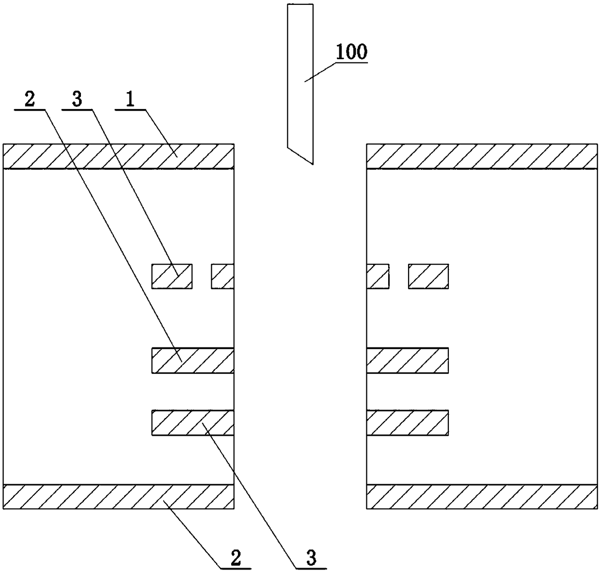
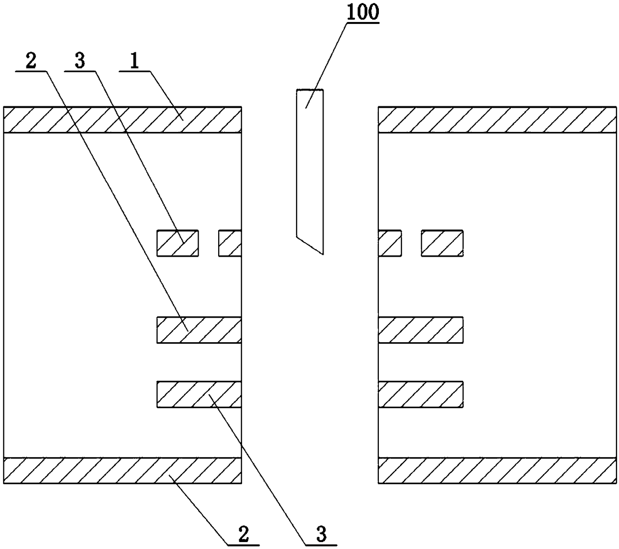
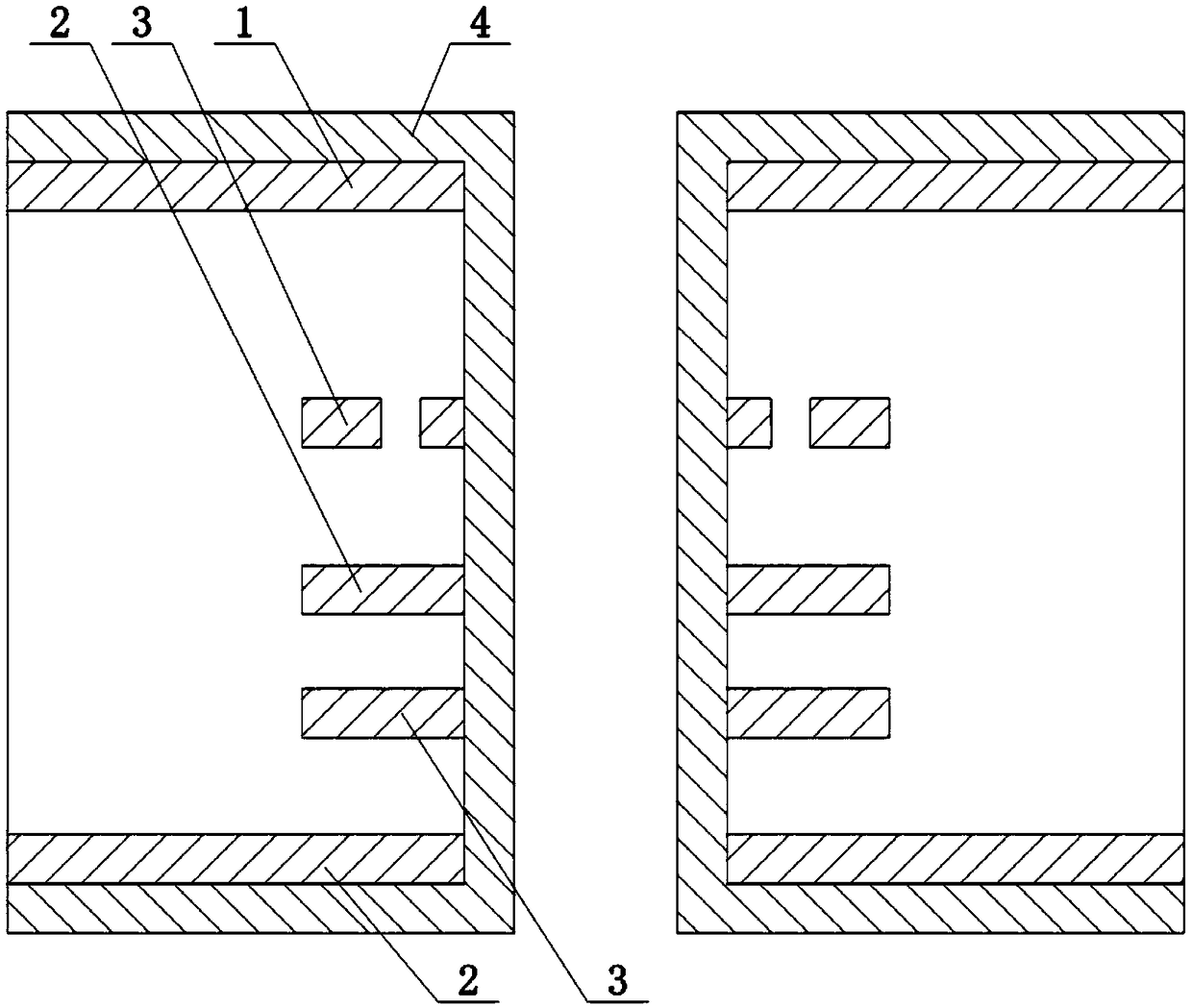
[0035] Such as Figure 1-Figure 4 As shown, the present invention provides a kind of PCB back drilling control method, comprises the following steps:

[0036] Step 1: Open a through hole on the PCB.

[0037] In this step, mechanical drilling is performed on the laminated PCB.

[0038] Step 2: Taking the drill-in surface of the back drill ...


PUM

PropertyMeasurementUnit
Diameteraaaaaaaaaa

Abstract

The invention belongs to the technical field of PCB manufacturing and discloses a PCB back drilling control method and a PCB. The PCB back drilling control method comprises steps: a through hole is opened in the PCB; with the drilling surface of back drilling as an upper surface, the distance L between an upper surface copper layer to a reference layer is measured; the PCB is electroplated; the thickness T of an electroplating layer on the upper surface copper layer is measured; and back drilling with a depth of L+T is carried out from one side of the upper surface copper layer on the throughhole. The PCB is manufactured by using the above PCB back drilling control method. The distance between the upper surface copper layer and the reference layer is measured before electroplating, the thickness of the electroplating layer on the upper surface copper layer is measured after electroplating, the sum of the two is used as a reference index for the depth of the back drilling, high-precision nondestructive detection on the dielectric thickness is realized, the back drilling depth can be accurately controlled in the case of back drilling, and the setting precision of a through hole residual pile can be improved.

Description

technical field [0001] The invention relates to the technical field of PCB preparation, in particular to a PCB backdrilling control method and a PCB. Background technique [0002] PCB (Printed Circuit Board), the Chinese name is printed circuit board, as a support for electronic components, it is an important electronic component. [0003] The via stubs in the PCB have a serious impact on signal transmission. At present, the impact of via stubs is mainly reduced by back drilling. Due to the influence of uneven thickness at different positions, conventional methods cannot achieve via stubs. High precision and stable control of piles requires the design of a conductive reference layer on the inner layer to detect the actual thickness of the medium. This method mainly requires the design of a conductive induction layer on the inner layer (special graphic design, and a back-drilling rig with special functions is required to cooperate with it. ), the graphic design of the inner ...

Claims


Application Information

Patent Timeline
IPC IPC(8): H05K3/00
CPCH05K3/0047H05K2203/0214H05K2203/163
Inventor 焦其正纪成光王洪府王小平
Owner DONGGUAN SHENGYI ELECTRONICS
Learn More