
IGBT device current waveform test board

A technology of current waveform and test board, which is applied in the field of test board structure, can solve problems such as inflexibility, high cost, and limited test range, and achieve the effects of improving measurement quality, solving influence, and reducing production and maintenance costs

Inactive Publication Date: 2019-01-04
上海卓弘微系统科技有限公司
View PDF0 Cites 0 Cited by
  • Summary
  • Abstract
  • Description
  • Claims
  • Application Information

AI Technical Summary

Problems solved by technology

[0007] 2. During the test, the whole process cannot be carried out in an ideal environment
Since the test signal is a high-frequency signal, any bad contact or inappropriate position of the equipment will have a great impact on the test results;
[0009] 4. The supporting equipment of the CDM test system currently used is mass-produced, and the cost is high, so it is not suitable for a small number of tests in small companies or laboratories
[0011] 1. High cost
In the actual environment, interference may come from various places. To achieve no interference, all-round protection must be achieved. All parts from the interference source to the transmission path must be protected. This not only ensures the accuracy of the results but also significantly increased costs;
[0012] 2. Due to the high cost of the existing industrial testing equipment, it is impossible to replace parts frequently, so its testing range is limited, and once damaged, it will cost a lot of manpower, material and financial resources to repair, which is not flexible enough;
[0013] 3. The current test equipment does not have a supporting structure specially designed to solve the influence of parasitic parameters, making the test results easily affected by parasitic parameters;
[0014] 4. The current test equipment has poor plasticity and cannot be flexibly modified according to test requirements

Method used


Image

  • IGBT device current waveform test board
  • IGBT device current waveform test board

Examples


Embodiment

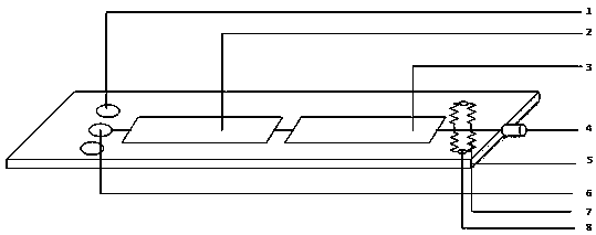
[0035] In an embodiment, the current discharge waveform of the CDM model detects a double-sided test board structure.

[0036] figure 1 and figure 2 The top and bottom views of the double-sided test board structure in the first embodiment of the present invention are respectively. Combining with this figure, it can be seen that the double-sided test board structure of this embodiment includes: a through-hole structure 1 with a fixing function on the back, which is used to install screws or other fixed devices; filter 2 for filtering out high-frequency interference; attenuator 3 for reducing current peaks to facilitate testing; grounding plate connected to metal socket 4 to connect the oscilloscope and test board through a coaxial cable; For connecting the grounding plate 5 of all parts, each module is assembled and has a grounding effect, and can be connected with other parts of the test system; pogo (pogo stick) probe 6, the part on the back of the test board is the probe b...


PUM


Abstract

The invention provides a test board structure for IGBT device current waveform detection. The invention aims to effectively capture a discharge current waveform consistent with a typical waveform in internationally accepted test specifications. The structure includes a pogo probe for directly contacting a discharge device, a filter for filtering out high-frequency interference, an attenuator for reducing current peaks to facilitate testing, a test resistor for converting current signals, and a grounding plate for connecting all the parts, wherein the filter and the attenuator are located on the grounding plate, and the grounding plate is connected with a metal socket so as to connect an oscilloscope, and the grounding plate contains a structure which enables a fixing effect and is used forconnecting the other parts of the test system.

Description

technical field [0001] The invention relates to the field of integrated circuits, in particular to a test board structure for current waveform detection in IGBT device testing. Background technique [0002] With the development of technology, IGBT devices are becoming more and more complex, and a small damage may lead to the scrapping of the entire device. Among the various electrostatic damages that the device may encounter, the CDM model is particularly noteworthy, not only because of its fast discharge speed, often making the protection circuit too late to turn on and unable to play a protective role, but also because of the current detection of the ESD current waveform of the CDM model. There is not yet a very robust test structure. At present, among various common ESD discharge models, HBM (Human Body Model) and MM (Machine Model) have their own corresponding relatively mature detection mechanisms, but CDM model detection is still relatively backward compared to the ab...

Claims


Application Information

Patent Timeline
IPC IPC(8): G01R19/00G01R29/02G01R29/04G01R31/00
CPCG01R19/0092G01R29/02G01R29/04G01R31/001
Inventor 沈立
Owner 上海卓弘微系统科技有限公司
Learn More