
Liquid crystal display panel

A liquid crystal panel, array substrate technology, applied in nonlinear optics, instruments, optics, etc., can solve the problems of signal deviation, affecting display uniformity, and inconsistent resistance of transmission signal lines

Inactive Publication Date: 2019-01-04
SHENZHEN CHINA STAR OPTOELECTRONICS TECH CO LTD
View PDF5 Cites 0 Cited by
  • Summary
  • Abstract
  • Description
  • Claims
  • Application Information

AI Technical Summary

Problems solved by technology

Due to the inconsistency of the length of the transmission signal line of each pixel, the resistance of the transmission signal line is also inconsistency, resulting in a deviation in the signal transmitted from the drive control signal to each pixel unit, which affects the uniformity of the display

Method used


Image

  • Liquid crystal display panel
  • Liquid crystal display panel
  • Liquid crystal display panel

Examples


Embodiment Construction

[0027] The problem to be solved by the present invention is to solve the problem of display deviation of the liquid crystal panel due to the inconsistency of the resistance of the signal transmission line. Embodiments of the present invention will be described in detail below in conjunction with the accompanying drawings.

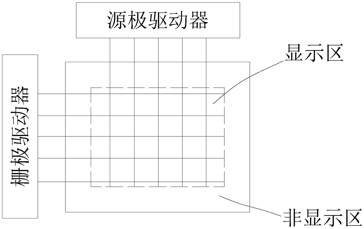
[0028] The liquid crystal panel structure of this embodiment includes a first substrate, a driver, a liquid crystal layer and a second substrate. Wherein the first substrate is an array substrate, and the array substrate includes a glass substrate and a gate electrode, an active layer, an insulating layer, a drain electrode / source electrode, a pixel electrode and a protective layer arranged on the glass substrate in sequence from bottom to top; The second substrate is a color filter substrate, including another glass substrate, a black matrix and a color resist set on the glass substrate, and a PS (Photo Spacer) layer set on the black matrix.

[0029] Such...


PUM


Abstract

The invention discloses a liquid crystal display panel, comprising a plurality of signal transmission lines used for transmitting signals between a driver and pixel electrodes of an array substrate, each signal transmission line is located in a non-display area of the array substrate and comprises a first signal circuit and a first resistance adjusting circuit, each first signal circuit is connected with at least one first resistance adjusting circuit in series, and in each signal transmission line, the sum of resistance values of the first signal circuit and the first resistance adjusting circuit connected with the first signal circuit in series is the same. The liquid crystal display panel disclosed by the invention has the advantages that resistance of each grid line is the same, and resistance of each source line is the same, so that no signal deviation is produced when the driver chip inputs a signal to each pixel electrode and all the signals are transmitted to the pixel electrodes, signal consistency can be maintained, the liquid crystal display panel shows uniformity, and display quality is better.

Description

technical field [0001] The present invention relates to the field of display technology, more specifically, to a liquid crystal panel. Background technique [0002] Existing TFT (Thin Film Transistor, Thin Film Transistor) LCD panel display, each pixel is controlled by a TFT switch, the gate of the TFT switch of each pixel is connected together to form a gate line, and the sources are connected together to form a signal line. When a certain pixel is selected, a voltage is applied to the gate of the TFT to make the TFT enter the conduction state, and at the same time, the display data is added to the source of the TFT through the signal line, and then reaches the drain of the TFT through the conduction TFT. An electric field is formed on the pixel to charge the liquid crystal material to realize the display effect. [0003] The gate and source drive signals are output from the drive circuit chip in the liquid crystal panel and input to the gate, source and drain of each pix...

Claims


Application Information

Patent Timeline
IPC IPC(8): G02F1/1362G02F1/1345
CPCG02F1/13452G02F1/136286
Inventor 周万亮
Owner SHENZHEN CHINA STAR OPTOELECTRONICS TECH CO LTD
Learn More