Manufacture method of display substrate
A technology for display substrates and substrates, which is used in semiconductor/solid-state device manufacturing, organic semiconductor devices, photovoltaic power generation, etc., and can solve the problems of uncontrollable laser ablation slope, high cost and low efficiency of back film lamination process, etc.
- Summary
- Abstract
- Description
- Claims
- Application Information
AI Technical Summary
Problems solved by technology
Method used
Image

Examples
Embodiment 1
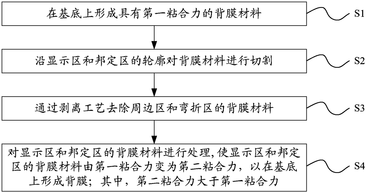
[0036] Such as figure 1 , 3 As shown in 7, this embodiment provides a method for preparing a display substrate, which is especially suitable for the preparation of a flexible OLED display substrate.
[0037] The preparation method specifically comprises the following steps:
[0038] S1, forming a back film material 51 with a first adhesive force on the substrate 4 .
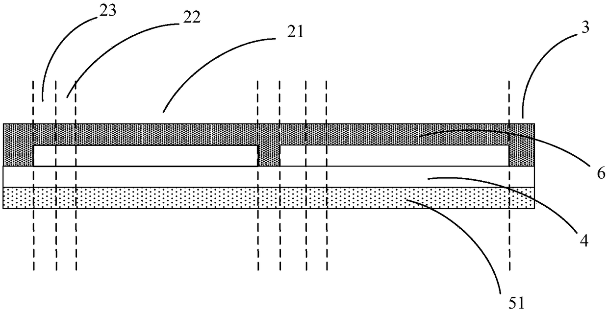
[0039] Among them, the substrate 4 is preferably made of flexible materials, such as polyimide. Specifically, in this step, the back film material 51 with the first adhesive force is formed on the non-display surface side of the substrate 4 (including the peripheral area 3 , the display area 21 , the bending area 22 and the bonding area 23 ). Wherein, the back film material 51 includes a back film 52 base material and a back film 52 adhesive material, and the back film 52 base material is attached to the base 4 through the back film 52 adhesive material. In this embodiment, the back film material 51 is a vari...
Embodiment 2
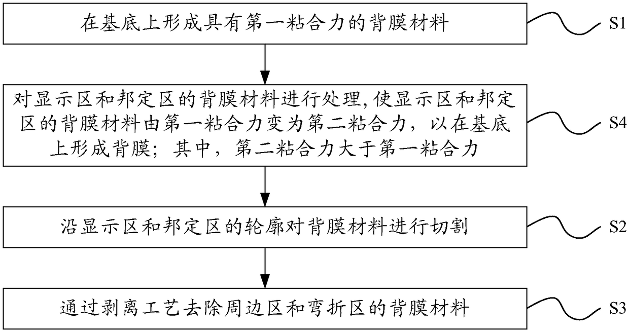
[0056] Such as figure 2 As shown, this embodiment provides a method for preparing a display substrate, which is basically the same as the method for preparing a display substrate provided in Embodiment 1.
[0057] In particular, in the preparation method of this embodiment, the back film material of the display area and the bonding area is treated first, so that the back film material of the display area and the bonding area changes from the first adhesive force to the second adhesive force. Adhesive force, then cut the back film material along the outline of the display area and the bonding area, and remove the back film material in the peripheral area and the bending area through a peeling process. That is, step S4 is executed first, and then steps S2 and S3 are executed.
[0058] Specifically, the back film material of the display area and the bonding area is treated first, so that the back film material of the display area and the bonding area changes from the first adhe...
Embodiment 3
[0062] Such as Figure 8 As shown, this embodiment provides an apparatus for preparing a display substrate, which is used to prepare a display substrate according to the method for preparing a display substrate provided in Embodiment 1.
[0063] The preparation device of the display substrate comprises: a back film material forming unit, a back film cutting unit, a back film removing unit, a back film adhesion increasing unit, and a substrate cutting unit. in,
[0064] The back film material forming unit is used for forming the back film material with the first adhesive force on the substrate.
[0065] The back film cutting unit is used to cut the back film material along the outline of the display area and the bonding area, so that the back film material in the display area is separated from the back film material in the peripheral area and the bending area, and the back film material in the bonding area It is separated from the back film material in the peripheral area and...
PUM
 Abstract
Description
Claims
Application Information
 - R&D
- Intellectual Property
- Life Sciences
- Materials
- Tech Scout
- Unparalleled Data Quality
- Higher Quality Content
- 60% Fewer Hallucinations
Browse by: Latest US Patents, China's latest patents, Technical Efficacy Thesaurus, Application Domain, Technology Topic, Popular Technical Reports.
© 2025 PatSnap. All rights reserved.Legal|Privacy policy|Modern Slavery Act Transparency Statement|Sitemap|About US| Contact US: help@patsnap.com