Objective table assembly and laser de-bonding device

A stage and debonding technology, applied in the direction of electrical components, electrical solid devices, semiconductor devices, etc., can solve the problems of increasing the pulling force of the tie rod, long scanning time, increasing the peeling time and difficulty of peeling the wafer and substrate

Pending Publication Date: 2021-12-28
北京中科镭特电子有限公司
View PDF0 Cites 0 Cited by
  • Summary
  • Abstract
  • Description
  • Claims
  • Application Information

AI Technical Summary

Problems solved by technology

However, since only one pull rod is connected to the suction cup, when the substrate and the wafer are separated, only the pulling force can be applied to the entire suction cup, so that the suction cup must be pulled after the laser scanning of the entire bonding layer is completed.
When the area of ​​the wafer and the substrate is large, it takes a long time to scan the entire bonding layer, so that the bonding layer that has just been heated by scanning and is in a molten state is condensed again, thereby bonding the wafer and the substrate again. Substrate
Therefore, the laser needs to scan the bonding layer back and forth multiple times to pull the entire suction cup through the pull rod to separate the substrate from the wafer, which not only increases the pulling force applied by the pull rod to the suction cup, but also increases the peeling time of the wafer and the substrate. and peeling difficulty

Method used


Image

  • Objective table assembly and laser de-bonding device
  • Objective table assembly and laser de-bonding device
  • Objective table assembly and laser de-bonding device

Examples


Embodiment Construction

[0031] In order to make the purpose, technical solutions and advantages of the embodiments of the present invention clearer, the technical solutions in the embodiments of the present invention will be clearly and completely described below in conjunction with the drawings in the embodiments of the present invention. Obviously, the described embodiments It is only some embodiments of the present invention, but not all embodiments. Based on the embodiments of the present invention, all other embodiments obtained by persons of ordinary skill in the art without making creative efforts belong to the protection scope of the present invention.

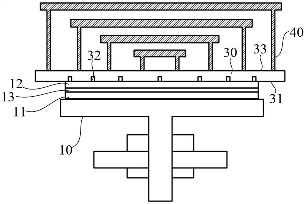
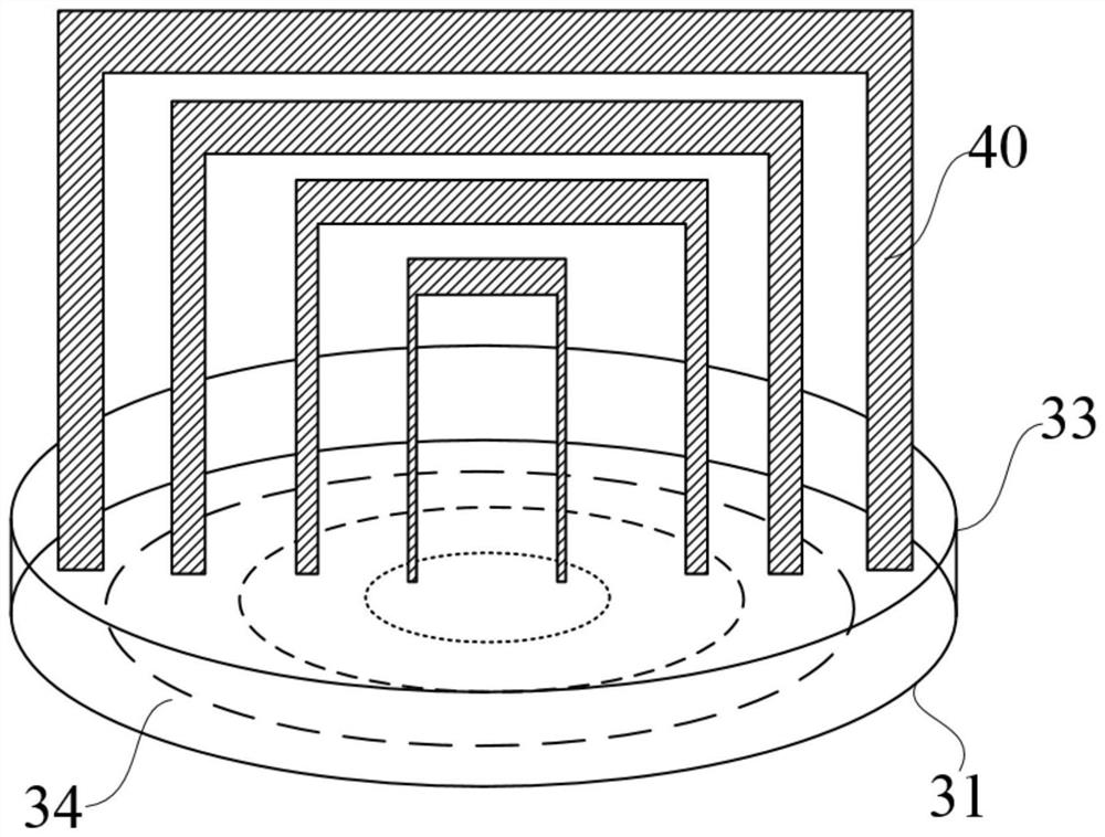
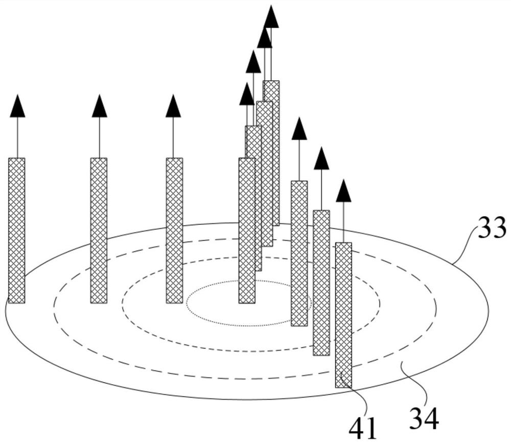
[0032] In order to facilitate the understanding of the stage assembly provided by the embodiment of the present invention, the application scene of the stage assembly provided by the embodiment of the present invention is firstly described below. During laser debonding of the parts to be debonded. Among them, refer to figure 1 , the bonded ...


PUM


Abstract

The invention provides an objective table assembly and a laser de-bonding device. The objective table assembly comprises an objective table, a suction cup and lifting assemblies. The first layer structure is fixed on the objective table. The suction cup is provided with an adsorption end face and a connecting end face, the adsorption end face is divided into at least three adsorption areas, and the adsorption areas comprise a circular adsorption area located in the center of the suction cup and at least two annular adsorption areas sequentially arranged from the circular adsorption area to the outside. The number of the lifting assemblies is at least three, and each lifting assembly is used for upwards pulling up the corresponding adsorption area after the bonding layer at the corresponding adsorption area position is heated by laser and subjected to phase change, so that the first layer structure and the second layer structure are separated at the corresponding adsorption area position. After part of the bonding layer area is scanned by laser, the corresponding adsorption area of the suction cup can be immediately lifted, so that the two layer structures at the adsorption area are separated, the situation that the bonding layer in the molten state is condensed and bonded again due to the fact that the part of the bonding layer area is heated by the laser is prevented, the stripping difficulty is reduced, the stripping time is shortened, and the stripping efficiency is improved.

Description

technical field [0001] The invention relates to the technical field of semiconductor manufacturing, in particular to an object stage assembly and a laser debonding device. Background technique [0002] In the manufacturing process of the chip, a large number of microelectronic devices are usually processed on the wafer by means of etching, deposition, polishing, etc. A wafer is a thin slice cut from a single crystal silicon ingot, and its thickness is usually between 0.3mm and 0.9mm, which shows that the thickness is very thin. Since the thickness of the wafer is relatively thin, and when various circuits are processed on the wafer, multiple times of etching, polishing, cleaning, etc. are required. Usually, the wafer is temporarily bonded to the substrate before processing. Afterwards, processes such as deposition and etching are carried out on the surface of the wafer to manufacture various microelectronic devices on the surface of the wafer. After the wafer processing is...

Claims


Application Information

Patent Timeline
Patent Type & Authority Applications(China)
IPC IPC(8): H01L21/67H01L21/683
CPCH01L24/799H01L21/6838H01L2224/7999
Inventor 张喆张紫辰李纪东张昆鹏侯煜张彪易飞跃杨顺凯
Owner 北京中科镭特电子有限公司
Why Eureka
Try Eureka