

A radio frequency power amplifier bias circuit
A bias circuit and radio frequency power technology, which is applied in the field of wireless communication, can solve the problems affecting the performance index of radio frequency power amplifiers, the sensitivity of bias voltage Vref changes, etc., and achieve the effect of reducing the amount of change and reducing the impact of performance indexes
- Summary
- Abstract
- Description
- Claims
- Application Information
AI Technical Summary
Problems solved by technology
Method used
Image

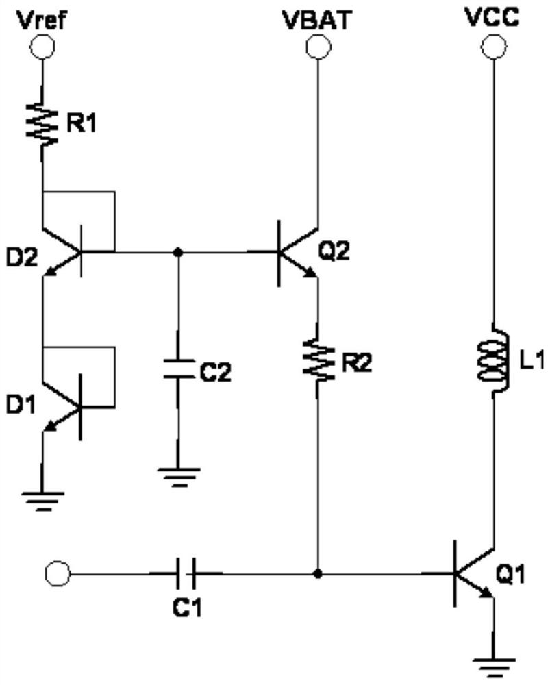


Examples
Embodiment 1
[0035] Embodiment 1 of the present application provides a bias circuit for a radio frequency power amplifier, such as figure 2 shown, the bias circuit includes:
[0036] A reference circuit module, a mirror circuit module, a ballast resistor, and a current adjustment circuit module, wherein,
[0037] The reference circuit module is used to provide a reference voltage for the mirror circuit module;
[0038] the mirror circuit module is used for generating the first current and the second current according to the reference voltage;
[0039] The current adjustment circuit module is used for adjusting the first current to the third current, so that the third current and the second current are superimposed to form the fourth current;
[0040] The fourth current passes through the ballast resistor R to bias the RF amplifier transistor Q1.
[0041] It should be noted that the essence of the current adjustment circuit module is to amplify the first current by a preset multiple, wh...
Embodiment 2
[0048] On the basis of the first embodiment, the second embodiment of the present application provides a more specific RF power amplifier bias circuit, such as image 3 As shown, the principle in this example is the same as that of the first embodiment, including: a reference circuit module, a mirror circuit module, a ballast resistor R, and a current adjustment circuit module.
[0049]In this embodiment, the mirror circuit module includes: a first transistor Q2 and a second transistor Q3; the reference circuit module includes: a third resistor R3, a fourth transistor D1, a fifth transistor D2 and a third transistor Two capacitors C2;
[0050] The base of the first transistor Q2 is connected to the base of the fifth transistor D2 as the output end of the reference circuit module as the input end of the mirror circuit module, the collector of the first transistor Q2 is connected to the power supply voltage Vbat, and the first transistor Q2 is connected to the power supply volta...
Embodiment 3
[0062] The third embodiment of the present application provides a more specific RF power amplifier bias circuit, such as Figure 5 shown. Similar to the second embodiment, the principle in this example is the same as that of the first embodiment, including: a reference circuit module, a mirror circuit module, a ballast resistor R, and a current adjustment circuit module.
[0063] In this embodiment, the mirror circuit module includes: a first transistor Q2 and a second transistor Q3; the reference circuit module includes: a third resistor R3, a fourth transistor D1, a fifth transistor D2 and a third transistor Two capacitors C2; the current adjustment circuit module includes: a third transistor Q4 and a first resistor R1, and may also include: a second resistor R2.
[0064] The base of the first transistor Q2 is connected to the base of the fifth transistor D2 as the output end of the reference circuit module as the input end of the mirror circuit module, the collector of the...
PUM
 Abstract
Description
Claims
Application Information