Protective film of conductive adhesive, circuit board and manufacturing method of display device

A manufacturing method and circuit board technology, applied in overvoltage protection, printed circuit manufacturing, printed circuit components, etc., can solve the problems of conductive adhesive failure, conductive adhesive protective film easy to fall off, etc., to increase adhesion and reduce tearing The effect of removing force and improving quality

Active Publication Date: 2019-01-04
BOE TECH GRP CO LTD +1
View PDF5 Cites 3 Cited by
  • Summary
  • Abstract
  • Description
  • Claims
  • Application Information

AI Technical Summary

Problems solved by technology

In order to stabilize the contact between the above two, it is necessary to use conductive adhesive to connect the two. Due to structural limitations, the area of ​​the exposed copper area is usually very small, and the area of ​​the conductive adhesive and the protective film is also small, so that the conductive adhesive protective film is easy to fall off, resulting in Conductive glue fails before connecting the two

Method used


Image

  • Protective film of conductive adhesive, circuit board and manufacturing method of display device
  • Protective film of conductive adhesive, circuit board and manufacturing method of display device
  • Protective film of conductive adhesive, circuit board and manufacturing method of display device

Examples


Embodiment Construction

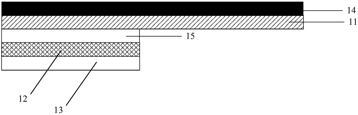
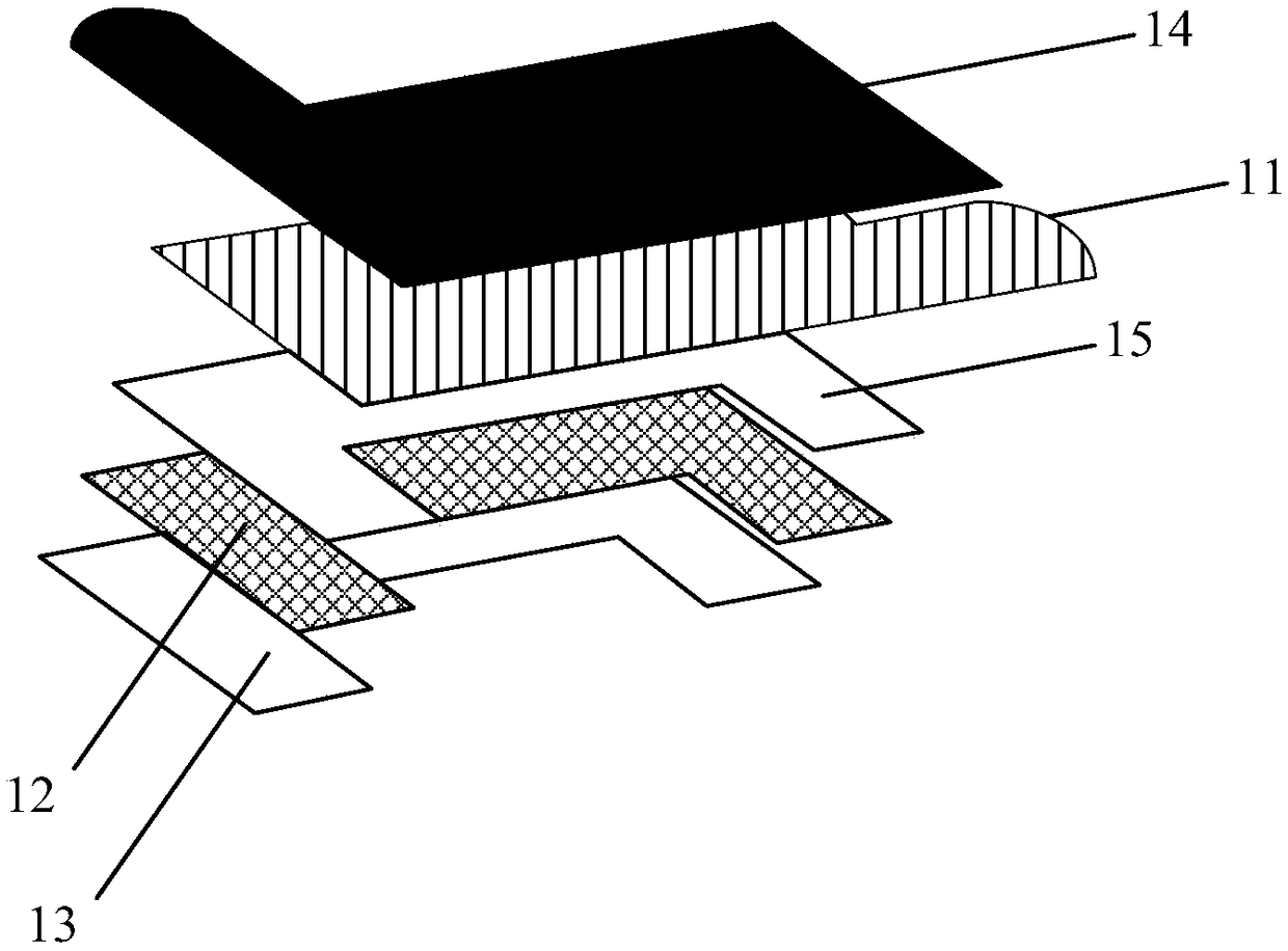
[0033] In the prior art, the exposed copper area is usually made on the circuit board to discharge static electricity, and the exposed copper area is electrically connected with the metal structure of the electronic device through conductive glue, so as to discharge the static electricity faster. Limited by the structure, the area of ​​the exposed copper area is small. In order to prevent the conductive adhesive from being torn off at the same time when the protective film on the conductive adhesive is torn off, the adhesion between the conductive adhesive and the protective film is small, but it is easy to cause the protective film to be damaged during the production process. Falling off, causing the conductive adhesive to lose its viscosity and conductive properties.

[0034] In order to solve the above technical problems, the present invention provides a protective film of conductive adhesive and a circuit board. The protective film includes a substrate and a photoreleasabl...


PUM


Abstract

The invention relates to the technical field of display, and discloses a protective film of a conductive adhesive, a manufacturing method of a circuit board and a display device. The protective film of the conductive adhesive comprises a photodetachable adhesive, such that the protective film is adhered to the circuit board through a photodetachable adhesive and a conductive adhesive, The adhesiveforce between the protective film and the circuit board is increased, and at least the peripheral area of the conductive adhesive is provided with a photodetachable adhesive, so that the protective film can be prevented from falling off from the conductive adhesive, the conductive adhesive is protected from being contaminated, and the conductive pattern and the static electricity releasing structure are reliably electrically connected through the conductive adhesive, thereby ensuring the static electricity derivation and improving the quality of the product. At that same time, when the display device is assemble, the photodetachable adhesive is irradiated with ultraviolet light, so that the photodetachable adhesive lose adhesion, the tearing force of the protective film is reduced, and the conductive adhesive is prevented from tearing off when the protective film is tear off, so that even if the adhesion between the protective film and the conductive adhesive is small, the protectivefilm is not easy to fall off.

Description

technical field [0001] The invention relates to the field of display technology, in particular to a protective film of conductive adhesive, a circuit board and a manufacturing method of a display device. Background technique [0002] In order to reduce the influence of static electricity on the signal characteristics of the display module, exposed copper areas are often left on the flexible circuit board. The exposed copper area is in contact with a certain metal structure of the display module in order to quickly discharge static electricity. In order to stabilize the contact between the above two, it is necessary to use conductive adhesive to connect the two. Due to structural limitations, the area of ​​the exposed copper area is usually very small, and the area of ​​the conductive adhesive and the protective film is also small, so that the conductive adhesive protective film is easy to fall off, resulting in The conductive glue fails before connecting the two. Contents...

Claims


Application Information

Patent Timeline
Patent Type & Authority Applications(China)
IPC IPC(8): H05K1/02H05K3/28
CPCH05K1/0213H05K3/281H05K2201/0195H05K1/0259H05K1/189H05K2201/09127H05K2201/10128H05K3/027H05K3/321H05K2201/09109
Inventor 赵磊王林松尹二涛崔志洋朱大华
Owner BOE TECH GRP CO LTD
Why Eureka
Try Eureka