A kind of manufacturing method of depletion mode field effect transistor

A field-effect transistor and manufacturing method technology, which is applied in the manufacture of semiconductor/solid-state devices, electrical components, circuits, etc., can solve the problems of difficult to precisely control the doping concentration of the channel region, serious lateral and vertical diffusion, and influence on ion distribution, etc. Achieve the effect of saving lithography levels, meeting different requirements and ensuring stability

Active Publication Date: 2020-08-11
江苏丽隽功率半导体有限公司
View PDF6 Cites 0 Cited by
  • Summary
  • Abstract
  • Description
  • Claims
  • Application Information

AI Technical Summary

Problems solved by technology

[0011] However, the above manufacturing method has the following disadvantages: (1), in order to realize the inversion of the channel, it is necessary to make a special N-type implantation region in the channel region, and photolithography is required, which is cumbersome
(2) Because the N-type implantation of the channel region is completed before the P-body region, the subsequent drive-in thermal process of the P-body region will affect the distribution of ions implanted in the channel region, and the lateral and vertical diffusion is relatively serious , the doping concentration of the channel region is difficult to precisely control

Method used


Image

  • A kind of manufacturing method of depletion mode field effect transistor
  • A kind of manufacturing method of depletion mode field effect transistor
  • A kind of manufacturing method of depletion mode field effect transistor

Examples


Embodiment Construction

[0053] The specific embodiments of the present invention will be further described below in conjunction with the accompanying drawings.

[0054] This application optimizes the manufacturing process of depletion-type field effect transistors and provides a new method of manufacturing depletion-type field-effect transistors. Please refer to Figure 9 The schematic diagram of the production process is shown, and the production method is as follows:

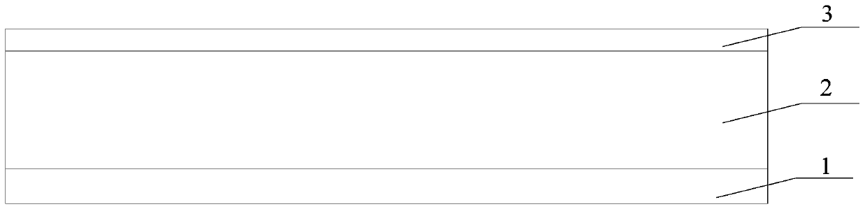
[0055] Step S01, providing a substrate 10, growing an epitaxial layer 20 on the substrate 10, the epitaxial layer 20 is doped with ions of a first conductivity type, where the first conductivity type ions are N-type ions or P-type ions, so that the epitaxial layer 20 Formed as an N-type epitaxial layer or a P-type epitaxial layer, the present application takes the substrate 10 as an N-type substrate and the epitaxial layer 20 doped with N-type ions to form an N-type epitaxial layer as an example.

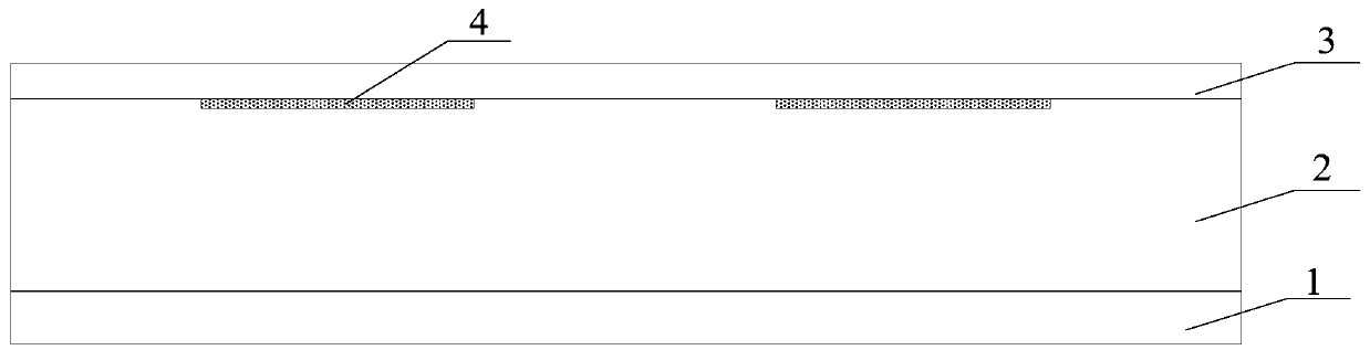
[0056] Step S02 , forming a thick ...


PUM

PropertyMeasurementUnit
thicknessaaaaaaaaaa
thicknessaaaaaaaaaa
thicknessaaaaaaaaaa

Abstract

The invention discloses a manufacturing method of a depletion type field effect transistor and relates to the technical field of semiconductors, the method sequentially fabricates a block-shaped discrete thick oxide layer on the epitaxial layer, a gate oxide layer and a discrete step-type polysilicon gate. Then make the body area, a local thick oxide layer and a step formed by a polysilicon gate electrode are use for ion implantation, as that ion implantation has different ability to penetrate the barrier with different thicknesses, ion doping in the channel region and ion doping in the source-drain region can be for simultaneously in the ion implantation process, and the requirements for ion concentration of the channel region and the source region can be met, the photolithography level is saved, and the fabrication step is simplified; In addition, since the doping in the channel region is fabricated after the body region is driven in, the ion doping distribution in the channel regionis not affected by the driving heat process in the body region, and the threshold voltage stability of the fabricated field effect transistor can be ensured.

Description

technical field [0001] The invention relates to the technical field of semiconductors, in particular to a manufacturing method of a depletion type field effect transistor. Background technique [0002] Field effect transistors mainly include enhanced field effect transistors and depletion type field effect transistors. At present, the conventional manufacturing process of the active area of ​​depletion type field effect transistors is as follows: [0003] 1. An N-type epitaxial layer 2 is grown on the surface of the N-type substrate 1, and a gate oxide layer 3 is formed on the upper surface of the N-type epitaxial layer 2. Please refer to figure 1 . [0004] 2. The N-type region 4 is formed in the N-type epitaxial layer 2 by photolithography and implantation process, please refer to figure 2 . [0005] 3. Form the polysilicon gate 5 through deposition, photolithography and etching processes, please refer to image 3 . [0006] 4. The P-body region 6 is formed by ion im...

Claims


Application Information

Patent Timeline
Patent Type & Authority Patents(China)
IPC IPC(8): H01L21/266H01L21/8234
CPCH01L21/266H01L21/823412H01L21/823418H01L21/823487
Inventor 范捷万立宏王绍荣
Owner 江苏丽隽功率半导体有限公司
Why Eureka
Try Eureka