A wafer fixing device and a wafer labeling apparatus for an integrated circuit

A wafer fixing and integrated circuit technology, applied in the direction of circuits, electrical components, electrical solid devices, etc., can solve the problems of low processing efficiency and yield, low automation rate of label pasting, inconvenient clamping and positioning, etc., to achieve processing High efficiency and processing yield, easy to replace label information, and increase the effect of processing range

Inactive Publication Date: 2019-01-11
吴美珍
View PDF0 Cites 1 Cited by
  • Summary
  • Abstract
  • Description
  • Claims
  • Application Information

AI Technical Summary

Problems solved by technology

The shortcomings of the existing equipment are: 1. A set of equipment can only operate on one size of wafer, and the wafer size is not compatible, resulting in high production costs; 2. The pre-printed label is pasted on the wafer, It is impossible to temporarily change the label, and the automation rate of label affixing is low; 3. The wafer loading and unloading is operated separately, resulting in low processing efficiency; 4. The wafer is small in size and inconvenient for clamping and positioning, resulting in low processing efficiency and yield

Method used


Image

  • A wafer fixing device and a wafer labeling apparatus for an integrated circuit
  • A wafer fixing device and a wafer labeling apparatus for an integrated circuit
  • A wafer fixing device and a wafer labeling apparatus for an integrated circuit

Examples


Embodiment 1

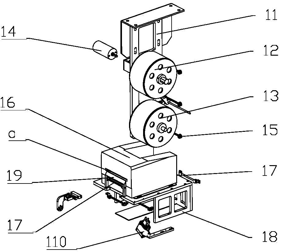
[0025] Such as Figure 7 , Figure 8 and Figure 9 The wafer fixing device shown includes a wafer adsorption mechanism 41 and a wafer stage mechanism 42; the wafer stage mechanism 42 is used to accept processed wafers, and its size can be adjusted to adapt to wafers of different sizes; The circular adsorption mechanism 41 is located at the center of the wafer stage mechanism 42, and is used to absorb the wafer fixed on the wafer stage mechanism 42, so as to ensure the stability during processing. The wafer fixture can be moved and fixed, which is convenient for wafer loading and unloading and labeling.

[0026] The wafer adsorption mechanism 41 includes a circular suction cup 411, a cylindrical optical shaft 412, a mounting plate 413, and a second cylinder 414; the cylindrical optical shaft 412 is fixed on the bottom of the circular suction cup 411, and the cylindrical optical shaft 412 is connected to the On the mounting plate 413, the circular suction cup 411 is provided ...

Embodiment 2

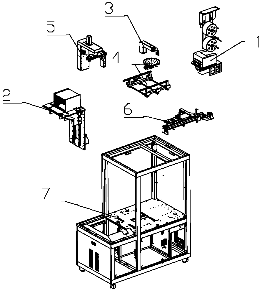
[0030] Such as Figure 1-Figure 11 The wafer labeling equipment for integrated circuits shown includes a frame 7 and a label feeding and discharging device 1 on it, a wafer feeding and discharging device 2, a label moving device 3, a wafer fixing device 4, a labeling detection device 5 and Wafer transfer device 6.

[0031] The wafer feeding and discharging device 2 is connected with the wafer fixing device 4 through the label moving device 3, and the wafer fixing device 4 is connected with the wafer feeding and discharging device 2. The labeling detection device 5 is located directly above the wafer fixing device 4. The position of the circular transfer device 6 corresponds to the wafer feeding and unloading device 2 and the wafer fixing device 4 .

[0032] The label feeding and discharging device 1 is used for blank label feeding, label spraying and recycling of waste paper. The wafer feeding and unloading device 2 is used for loading wafers to be labeled and unloading fini...


PUM


Abstract

The invention relates to the technical field of integrated circuits. A wafer fixing device comprising a wafer adsorption mechanism and a wafer stage mechanism. The wafer stage mechanism is used for receiving the processed wafer. The wafer suction mechanism is located in the center of the wafer stage mechanism for sucking the wafer fixed on the wafer stage mechanism. The wafer fixing device has theadvantages of convenient and stable wafer positioning, and is suitable for wafers of different sizes.

Description

technical field [0001] The invention relates to the technical field of integrated circuits, in particular to wafer labeling equipment. Background technique [0002] Wafer refers to the silicon wafer used in the production of silicon semiconductor integrated circuits. Millions of transistors can be etched on the wafer through a special process, and it is widely used in the manufacture of integrated circuits. After the wafer processing is completed, a label needs to be attached to it. The existing labeling operation method is: first fix the wafer, then paste the pre-printed label on the wafer, remove the labeled wafer and continue Load the wafers to be labeled and repeat. The shortcomings of the existing equipment are: 1. A set of equipment can only operate on one size of wafer, and the wafer size is not compatible, resulting in high production costs; 2. The pre-printed label is pasted on the wafer, It is impossible to temporarily change the label, and the automation rate of...

Claims


Application Information

Patent Timeline
Patent Type & Authority Applications(China)
IPC IPC(8): H01L21/683H01L21/687H01L21/67
CPCH01L21/6838H01L21/67282H01L21/68721H01L2223/54493
Inventor 吴美珍
Owner 吴美珍
Why Eureka
Try Eureka