Multifunctional semiconductor resistance tester

A resistance tester, semiconductor technology, applied in grounding resistance measurement, high resistance measurement, parts of electrical measuring instruments, etc., can solve problems such as unstable side-view instrument lifting, difficult to observe the host, no storage box, etc. , to achieve the effect of improving portability, avoiding insufficient contact, and facilitating the mastery of lifting distance

Inactive Publication Date: 2019-01-15
JIANGSU NEPES SEMICON
View PDF0 Cites 0 Cited by
  • Summary
  • Abstract
  • Description
  • Claims
  • Application Information

AI Technical Summary

Problems solved by technology

[0004] The purpose of the present invention is to provide a multi-functional semiconductor resistance tester to solve the problems of the existing semiconductor side-view instrument, such as unstable lifting, no storage box, difficult to observe due to weak light, and unportable host.

Method used


Image

  • Multifunctional semiconductor resistance tester
  • Multifunctional semiconductor resistance tester

Examples


Embodiment Construction

[0019] The following will clearly and completely describe the technical solutions in the embodiments of the present invention with reference to the accompanying drawings in the embodiments of the present invention. Obviously, the described embodiments are only some, not all, embodiments of the present invention. Based on the embodiments of the present invention, all other embodiments obtained by persons of ordinary skill in the art without making creative efforts belong to the protection scope of the present invention.

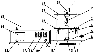
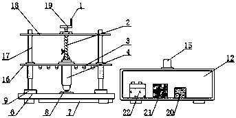
[0020] see figure 1 with figure 2 , the present invention provides a technical solution: a multifunctional semiconductor resistance tester, including a host 12 to analyze the measurement data, a detector interface 10, a function button 11, a power button 13 and Display screen 14, display screen 14 shows resistance value, power button 13 is positioned at the side of display screen 14, and the top of power button 13 is provided with detector interface 10, conn...


PUM


Abstract

The invention discloses a multifunctional semiconductor resistance tester, which comprises a mainframe. A detector interface, function buttons, a power button and a display screen are arranged on theouter wall of one side of the mainframe; the power button is located on one side of the display screen, and the detector interface is arranged above the power button; the function buttons are arrangedabove the detector interface; the top end of the mainframe is fixedly connected with a handle; an AD converter, an STC89C52RC single chip microcomputer and a storage battery are arranged inside the mainframe; the AD converter is arranged on one side of the STC89C54RC single chip microcomputer and the storage battery is arranged on the other side of the STC89C52RC single chip microcomputer; and atest board is arranged on one side of the mainframe. According to the multifunctional semiconductor resistance tester in the invention, a lifting platform is supported and fixed through four support rods, thereby avoiding inaccurate measurement data caused by insufficient contact of a detector probe; a clear view can be provided through an LED lamp installed on the lower end of the lifting platform, thereby bringing convenience for an operator to grasp the lifting distance, and improving the operation accuracy.

Description

technical field [0001] The invention belongs to the technical field of resistance testers, and in particular relates to a multifunctional semiconductor resistance tester. Background technique [0002] The resistance tester is an indispensable tool for electrical safety inspection and grounding project completion acceptance. Including ground resistance tester, insulation resistance tester, DC resistance tester, surface resistance tester and loop resistance tester. The loop resistance measuring instrument (transformer loop resistance tester) is suitable for testing the contact resistance value of the main contact of the high and low voltage switch, the DC resistance value of the high and low voltage cable line, etc. The intelligent loop resistance tester adopts 100A constant current output. The highest output voltage is up to 10V (2-3 times that of conventional instruments), and the test line with thin surface can be used, which greatly reduces the labor intensity of on-site...

Claims


Application Information

Patent Timeline
Patent Type & Authority Applications(China)
IPC IPC(8): G01R1/04G01R1/02G01R27/02G01R27/20G05B19/042
CPCG01R1/04G01R1/02G01R1/0425G01R27/025G01R27/20G05B19/042G05B19/0423G05B2219/21137G05B2219/2604
Inventor 黄涛袁泉孙健张慧朱威莉韩伟
Owner JIANGSU NEPES SEMICON
Why Eureka
Try Eureka