Micro LED display panel, manufacturing method thereof and display device

A technology for display panels and manufacturing methods, applied in semiconductor/solid-state device manufacturing, semiconductor devices, electrical components, etc., can solve problems such as complex processes, achieve the effects of simplifying the process, avoiding damage, and reducing the difficulty of the process

Active Publication Date: 2019-02-01
SHANGHAI TIANMA MICRO ELECTRONICS CO LTD
View PDF6 Cites 15 Cited by
  • Summary
  • Abstract
  • Description
  • Claims
  • Application Information

AI Technical Summary

Problems solved by technology

[0003] Among them, the Micro LED display integrates the technical characteristics of TFT-LCD (thin film transistor-liquid crystal display, thin film transistor liquid crystal display) and LED display. Then transfer the Micro LED from the initial growth substrate to the circuit substrate. One of the difficulties in the development of Micro LED technology lies in the transfer process of Micro LED. Currently, the process of transferring Micro LED chips to the circuit substrate is complicated.

Method used


Image

  • Micro LED display panel, manufacturing method thereof and display device
  • Micro LED display panel, manufacturing method thereof and display device
  • Micro LED display panel, manufacturing method thereof and display device

Examples


Embodiment Construction

[0035] The following will clearly and completely describe the technical solutions in the embodiments of the present invention with reference to the accompanying drawings in the embodiments of the present invention. Obviously, the described embodiments are only some, not all, embodiments of the present invention. Based on the embodiments of the present invention, all other embodiments obtained by persons of ordinary skill in the art without making creative efforts belong to the protection scope of the present invention.

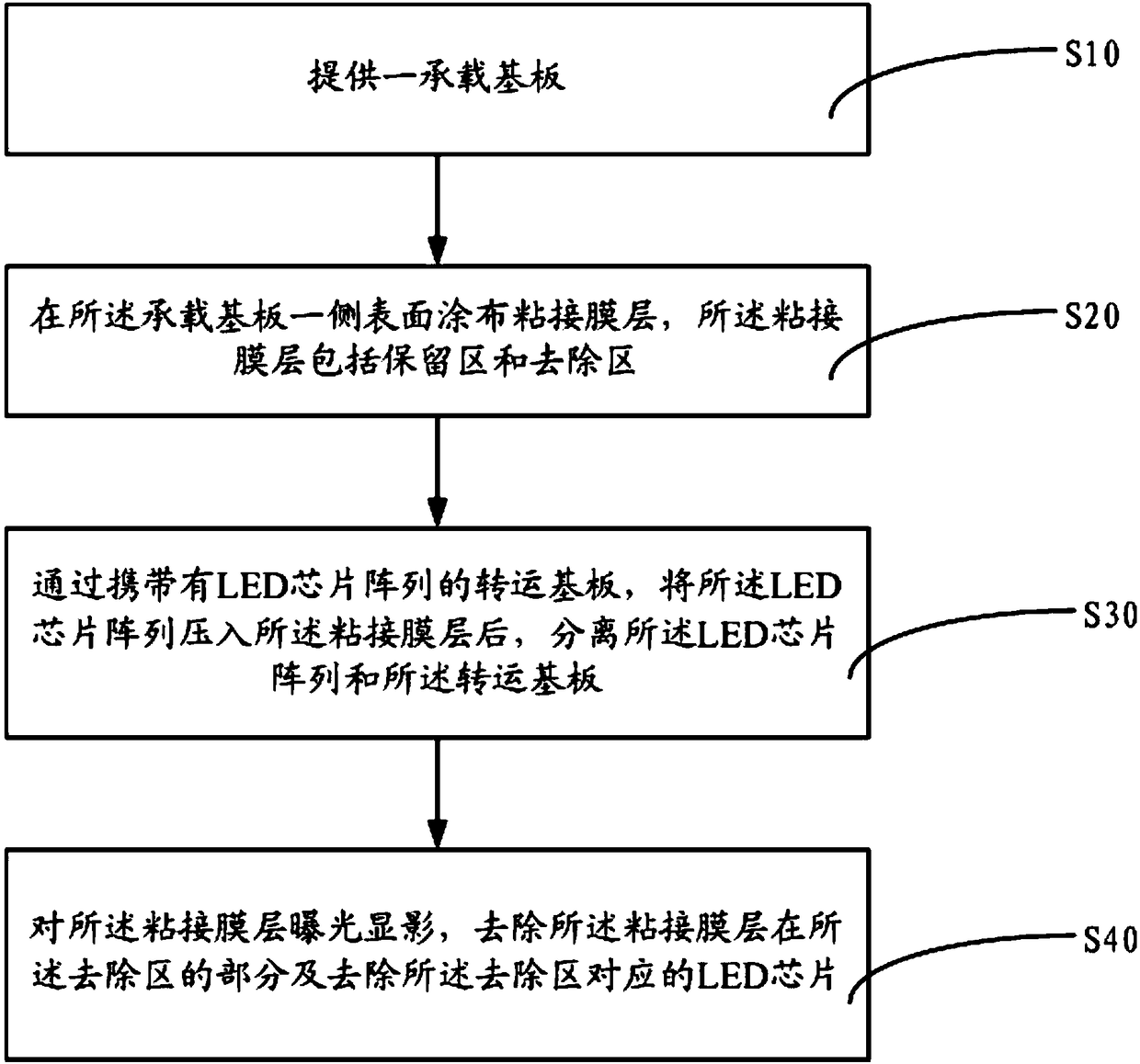
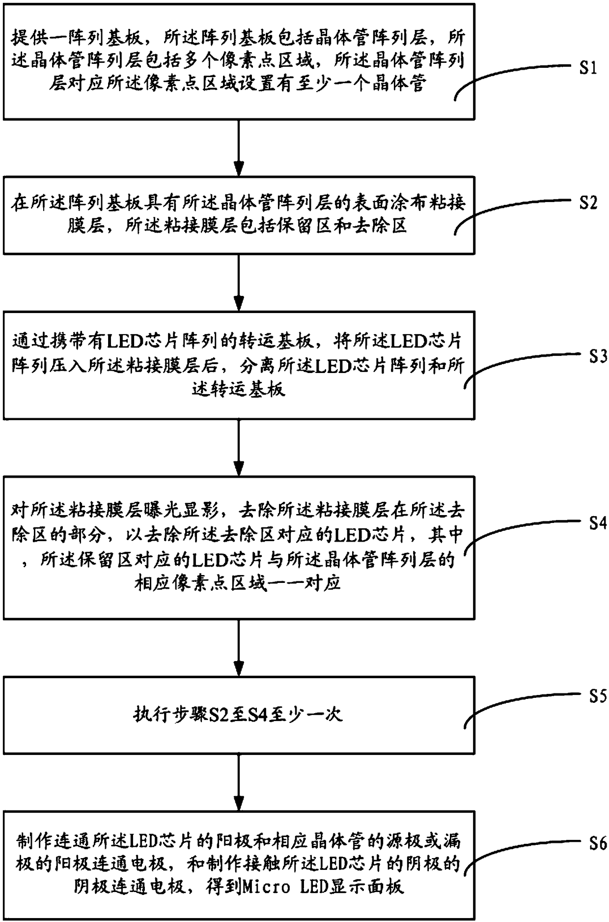
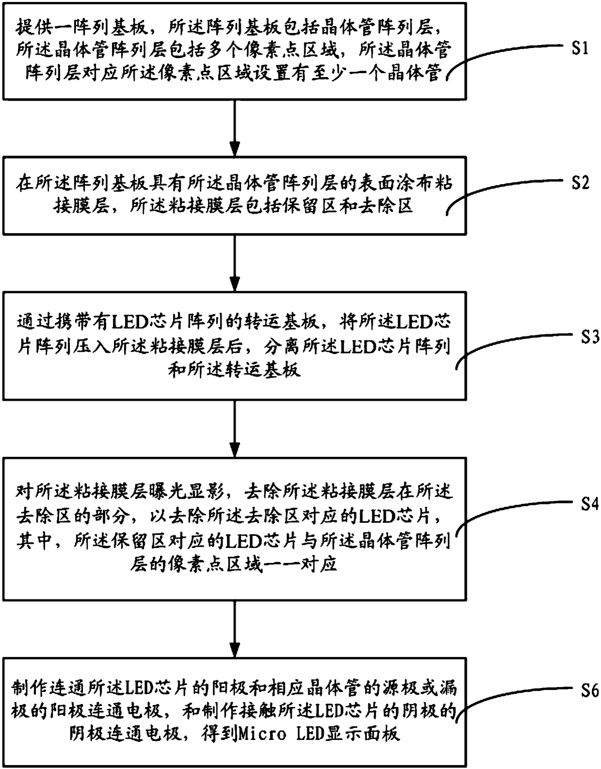
[0036] As mentioned in the background technology, the Micro LED display integrates the technical characteristics of TFT-LCD and LED display. One of the difficulties in the development of Micro LED technology is the transfer process of Micro LED. Currently, the process of transferring Micro LED chips to circuit substrates is complicated.

[0037] Based on this, the embodiment of the present application provides a Micro LED display panel, a manufacturing method ...


PUM


Abstract

The invention discloses a Micro LED display panel, a manufacturing method thereof and a display device. It is only required to press an LED chip array into a bonding film layer when the LED chip arrayis transferred, the LED chip array is bonded onto a bearing substrate or an array substrate via the bonding film layer, and an unnecessary part of the bonding film layer is removed to remove unnecessary LED chips and thus complete transfer. All chips in the LED chip array are welded to the substrate one by one needless of a welding manner, The Micro LED display panel manufacturing technology is simplified, the technical difficulty of the Micro LED display panel is reduced, influence of high temperature of the welding technology on the LED chip is avoided, and the LED chips are avoided from damage in the transfer process.

Description

technical field [0001] The present invention relates to the field of display technology, and more specifically, to a Micro LED display panel, a manufacturing method thereof, and a display device. Background technique [0002] Light Emitting Diode (LED) is an optoelectronic semiconductor element that can convert current into a specific wavelength range. Its light-emitting principle is the energy difference between electrons moving between n-type semiconductors and p-type semiconductors, releasing energy in the form of light , so light-emitting diodes are called cold light sources, which have the advantages of low power consumption, small size, high brightness, easy matching with integrated circuits, and high reliability, and are widely used as light sources. Moreover, with the maturity of LED technology, the technology of directly using LEDs as self-luminous display dot pixels of LED displays or Micro LED (ie, micro LED) displays is gradually being widely used. [0003] Amon...

Claims


Application Information

Patent Timeline
Patent Type & Authority Applications(China)
IPC IPC(8): H01L27/15H01L33/00
CPCH01L27/156H01L33/0093H01L25/0753H01L33/504H01L33/508H01L33/56H01L25/167H01L33/62H01L33/505H01L33/42H01L2933/0066H01L2933/005H01L21/6835H01L2221/68354H01L2221/68368H01L2224/97H01L2224/83855H01L2224/94H01L2224/83191H01L2224/8393H01L2224/83931H01L2224/821H01L2224/24105H01L2224/24145H01L2224/95H01L2224/95136H01L2224/2919H01L24/83H01L24/29H01L24/32H01L24/24H01L24/95H01L24/94H01L2224/83H01L2924/00014H01L2224/82H01L2924/0665H01L2224/32145H01L2933/0041H01L33/52
Inventor 符鞠建刘刚
Owner SHANGHAI TIANMA MICRO ELECTRONICS CO LTD
Why Eureka
Try Eureka