

Formation method of semiconductor structure
A technology of semiconductor and isolation structure, which is applied in the field of semiconductor structure formation to achieve the effect of simplifying process flow, improving production efficiency and improving performance
- Summary
- Abstract
- Description
- Claims
- Application Information
AI Technical Summary
Problems solved by technology
Method used
Image


Examples
Embodiment Construction
[0028] As mentioned in the background, the existing method for fabricating polysilicon dummy gates needs to be improved. Now analyze and illustrate in conjunction with specific embodiment.
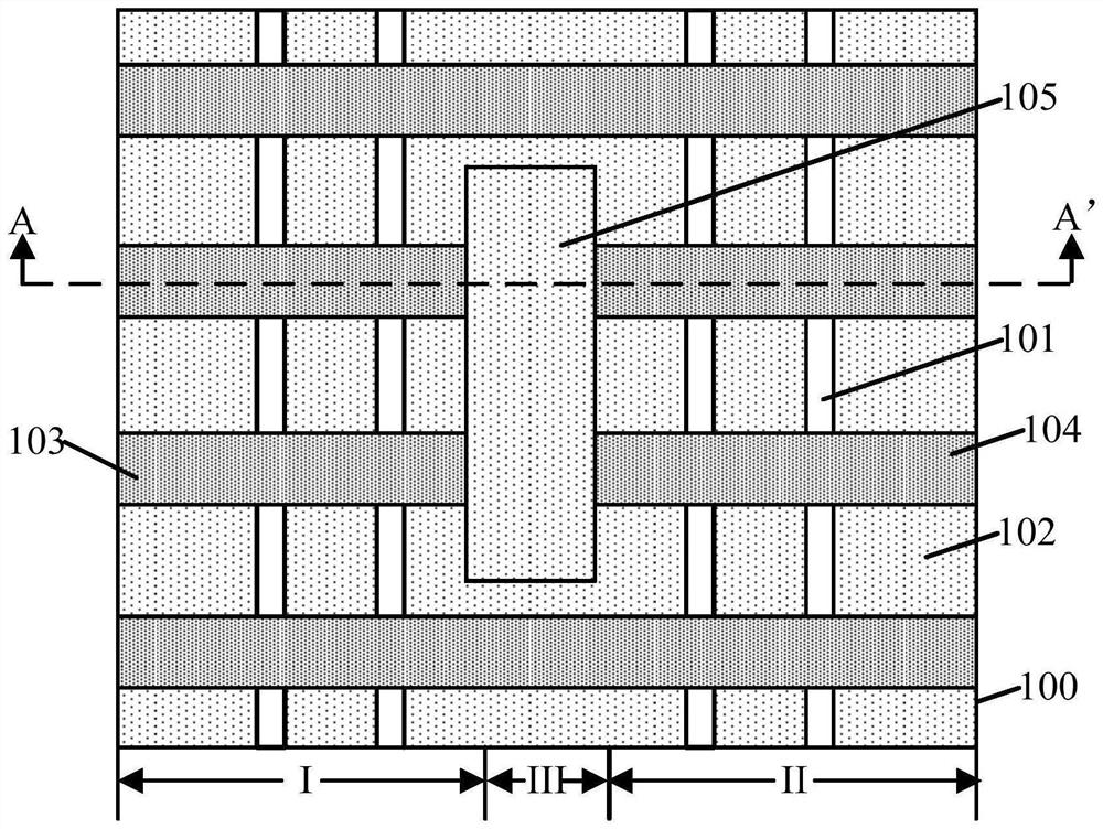
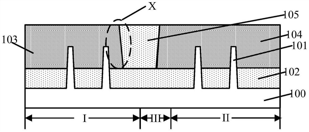
[0029] figure 1 and figure 2 They are respectively a top view and a cross-sectional schematic diagram of a semiconductor structure in an embodiment.
[0030] Please refer to figure 1 and figure 2 , figure 1 for figure 2 top view of figure 2 for figure 1 A schematic cross-sectional structure along the section line AA', wherein the section line AA' extends along the direction of the dummy gate structure, including: a substrate 100 including a first region I, a second region II and an isolation region III, the isolation region III is located between the first region I and the second region II, the first region I and the second region II have a fin structure 101; the first dielectric layer 102 on the substrate 100, The first dielectric layer 102 is located on the sidewall of the f...
PUM
 Abstract
Description
Claims
Application Information