Disconnection repair method, substrate and display device

A repair method and substrate technology, applied in nonlinear optics, instruments, conductors, etc., can solve the problems of long repair time, affecting the performance of pixel units around the disconnected area, and high repair cost

Active Publication Date: 2021-09-10
BOE TECH GRP CO LTD
View PDF14 Cites 0 Cited by
  • Summary
  • Abstract
  • Description
  • Claims
  • Application Information

AI Technical Summary

Problems solved by technology

[0004] In order to solve the problems of high repair cost and long repair time in the prior art, and affect the performance of pixel units around the broken line area, the embodiment of the present invention provides a broken line repair method, a substrate and a display device

Method used


Image

  • Disconnection repair method, substrate and display device
  • Disconnection repair method, substrate and display device
  • Disconnection repair method, substrate and display device

Examples


Embodiment Construction

[0040] In order to make the object, technical solution and advantages of the present invention clearer, the implementation manner of the present invention will be further described in detail below in conjunction with the accompanying drawings.

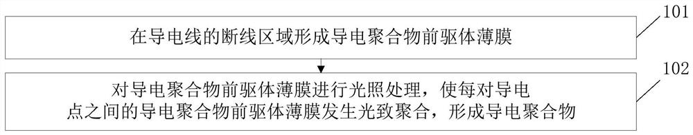
[0041] figure 1 It is a flow chart of a disconnection repair method provided by an embodiment of the present invention, see figure 1 , the method includes:

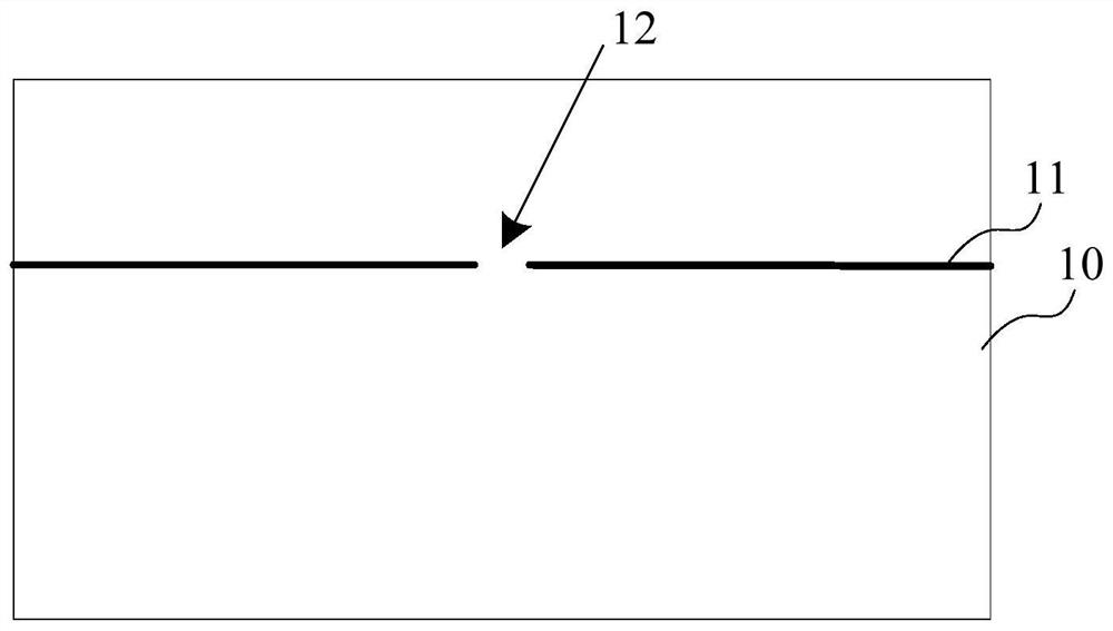
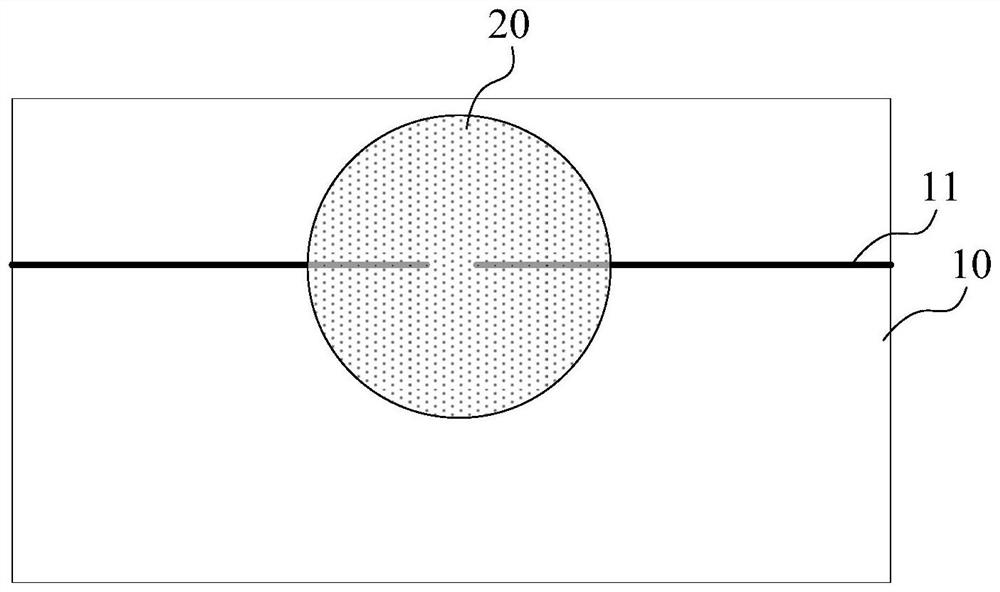
[0042] Step 101: forming a conductive polymer precursor film in the disconnected area of ​​the conductive line, the disconnected area includes at least one pair of conductive points, each pair of conductive points includes two conductive points disconnected from each other, the conductive polymer precursor film and at least A pair of conductive point contacts.

[0043] In the embodiment of the present invention, the conductive lines may be signal lines or electrodes on the substrate in the display panel, usually made of metal or indium tin oxide (Indium tin oxide, ITO), such as ...


PUM


Abstract

The invention discloses a disconnection repair method, a substrate and a display device, belonging to the field of displays. The method includes: forming a conductive polymer precursor film in a broken line area of ​​the conductive line, the broken line area includes at least one pair of conductive points, each pair of conductive points includes two conductive points disconnected from each other, and the conductive polymer precursor film Contacting at least one pair of conductive points; performing light treatment on the conductive polymer precursor film, so that the conductive polymer precursor film between each pair of conductive points undergoes photopolymerization to form a conductive polymer. The conductive polymer precursor film is photopolymerized by light to form a conductive polymer, so that a conductive polymer line is generated between each pair of conductive points, and each pair of conductive points is connected to realize circuit repair without using laser chemistry. Vapor deposition, low repair cost and short repair time, will not affect the performance of pixel units around the disconnected area.

Description

technical field [0001] The invention relates to the field of displays, in particular to a disconnection repair method, a substrate and a display device. Background technique [0002] Thin Film Transistor-Liquid Crystal Display (TFT-LCD) uses the change of the electric field intensity on the liquid crystal molecular layer loaded between the upper and lower substrates to change the orientation of the liquid crystal molecules, thereby controlling the intensity of light transmission. A display device to display images. A liquid crystal display panel generally includes an array substrate, a color filter (Color Filter, CF) substrate, and a layer of liquid crystal molecules filled in a liquid crystal cell formed by the two substrates. A large number of pixel units are arranged in an array on the array substrate, and each pixel unit includes a TFT; usually, the TFTs of each row of pixel units are connected to a horizontally arranged gate line, and the gate line is used to control t...

Claims


Application Information

Patent Timeline
Patent Type & Authority Patents(China)
IPC IPC(8): G02F1/1362G02F1/13
CPCG02F1/1309G02F1/136259G02F1/136263H01L27/124H01L21/76892G02F2202/022G02F2202/16H01B1/127C08F2/48H01L21/31133H01L21/76883H01L27/1259
Inventor 谢蒂旎李伟
Owner BOE TECH GRP CO LTD
Why Eureka
Try Eureka