

Layout structure for saving chip area and a preparation method thereof
A layout structure and chip area technology, applied in special data processing applications, instruments, electrical digital data processing, etc., can solve problems such as large chip area, and achieve the effect of reducing chip cost, reducing cost, and saving area
- Summary
- Abstract
- Description
- Claims
- Application Information
AI Technical Summary
Problems solved by technology
Method used
Image

Examples
Embodiment 1
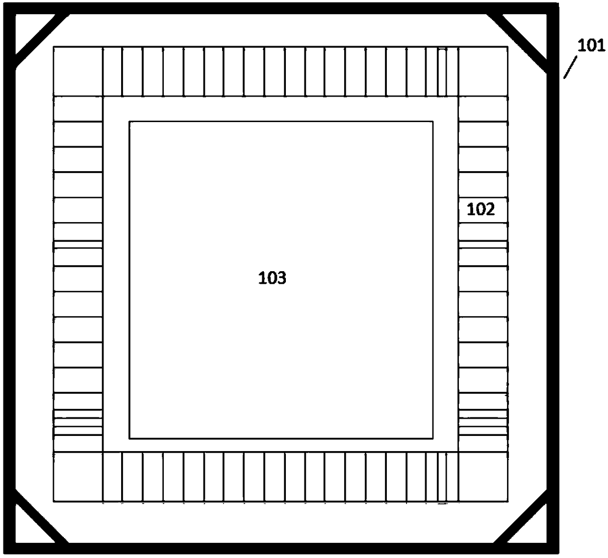
[0026] Embodiment 1, in the implementation process of chip physical design, this technical solution increases the realization of the core module of irregular shape, cuts off the corner area of 75umx75um in the two core modules, and then increases the length or width of the core module of irregular shape , so as to ensure that the layout area of the overall irregular shape core module remains unchanged, and then the irregular shape core module can be physically realized as the ordinary core module, and then the two core modules with the corner area of 75umx75um cut off are placed on the two sides of the chip One corner, the cutting position is placed relative to the sealring of the chip outer frame, and the side border of the sealring can be indented by at least 75um, so that the border on the side of the sealring1 can be indented without changing the size of the core logic area of the chip. The inner indentation is at least 75um, so as to reduce the chip area by changin...
Embodiment 2
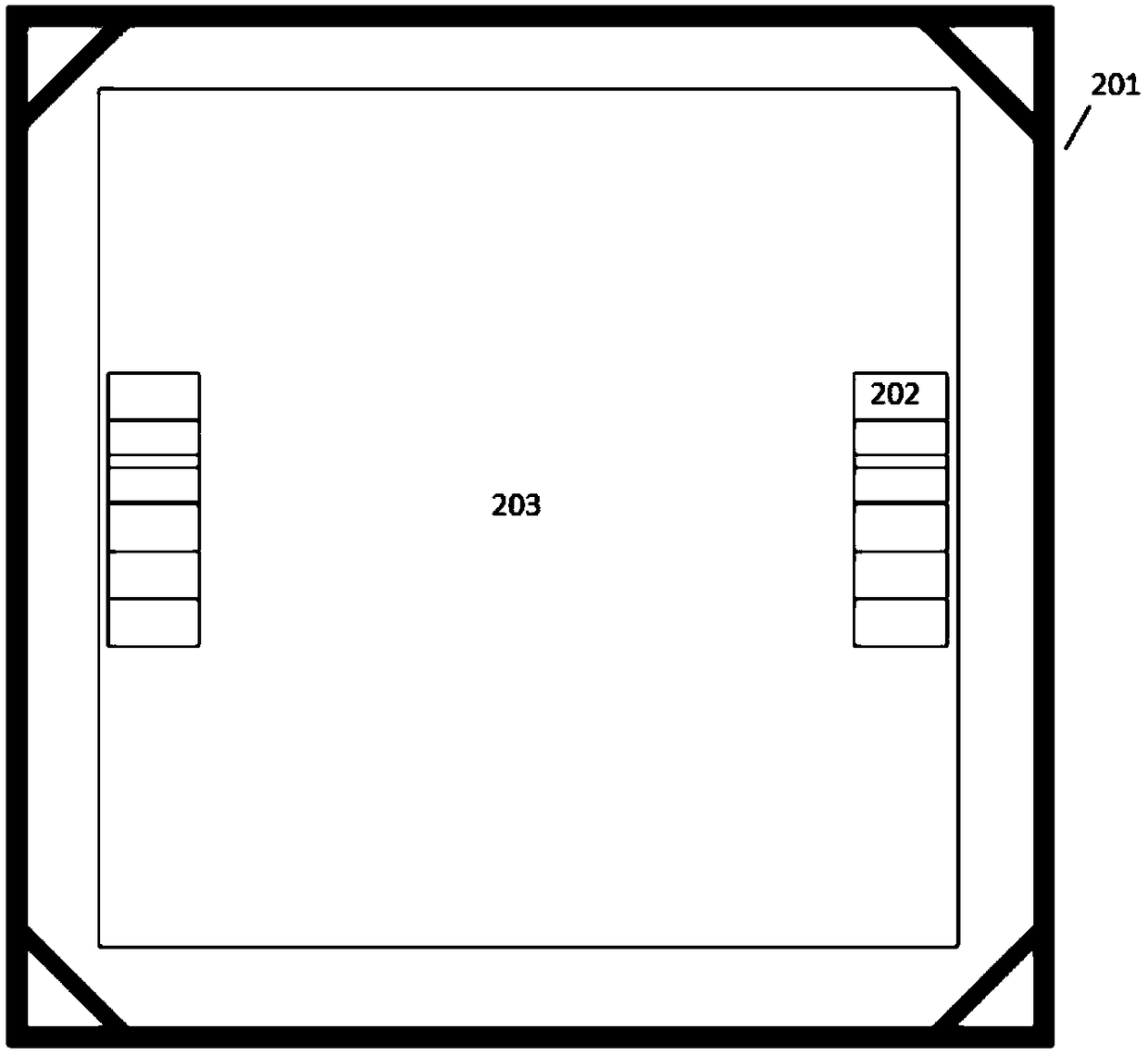
[0027] Embodiment 2, increase the realization of irregularly shaped core modules, cut off the corner area of 75umx75um in the three core modules, and then increase the length or width of the irregularly shaped core modules, so as to ensure the layout of the overall irregularly shaped core modules The area remains the same, and then the irregular shape core module can be physically realized like the ordinary core module, and then three core modules with the corner area of 75umx75um cut off are placed on the three corners of the chip, and the cut position is placed relative to the sealring of the chip outer frame , so that without changing the size of the core logic area of the chip, the borders on both sides of the sealring can be indented by at least 75um, thereby reducing the chip area by changing the chip structure layout. The chip area is reduced by cutting off the corner of the core module and placing the cut corner relative to the seal ring of the chip outer frame, a...
Embodiment 3
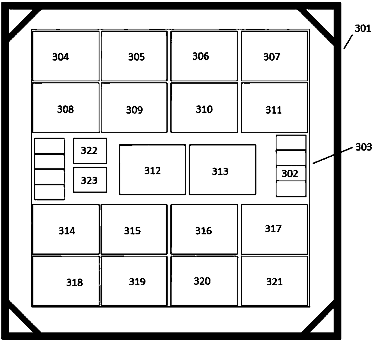
[0028] Embodiment 3, increase the realization of the core module of irregular shape, cut off the corner area of 75umx75um in the four core modules, and then increase the length or width of the core module of irregular shape, thereby ensuring the layout of the overall irregular shape core module The area remains the same, and then the irregular-shaped core module can be physically realized as the ordinary core module, and then the four core modules with the corner area of 75umx75um cut off are placed on the four corners of the chip, and the cut-off position is placed relative to the sealring401 of the chip outer frame , so that without changing the size of the core logic area of the chip, the border of the sealring 401 can be indented by at least 75um, thereby reducing the chip area by changing the chip structure layout. The chip area is reduced by cutting off corners of the core module and placing the cut corners relative to the sealring 401 of the chip outer frame, and t...
PUM
 Abstract
Description
Claims
Application Information