Chip package structure easy to cool and package method of chip package structure

A technology of chip packaging structure and heat sink, which is applied in the direction of electrical components, electric solid devices, circuits, etc., can solve the problems of unreasonable design of chip packaging structure, inability to dissipate heat and cool down in time, and internal air circulation, etc., to achieve reasonable structural design, The effect of large heat dissipation space and accelerated heat dissipation speed

Active Publication Date: 2019-02-15
常熟市华通电子有限公司
View PDF4 Cites 16 Cited by
  • Summary
  • Abstract
  • Description
  • Claims
  • Application Information

AI Technical Summary

Problems solved by technology

[0004] The technical problem solved by the present invention is to overcome the defects of unreasonable design of chip packaging structure in the prior art, small space for heat dissipation, no circulation of internal air, and inability to dissipate heat and cool down in time, and provide a chip packaging structure and packaging method that is easy to dissipate heat

Method used


Image

  • Chip package structure easy to cool and package method of chip package structure
  • Chip package structure easy to cool and package method of chip package structure

Examples


Embodiment Construction

[0022] The following will clearly and completely describe the technical solutions in the embodiments of the present invention with reference to the accompanying drawings in the embodiments of the present invention. Obviously, the described embodiments are only some, not all, embodiments of the present invention. Based on the embodiments of the present invention, all other embodiments obtained by persons of ordinary skill in the art without making creative efforts belong to the protection scope of the present invention.

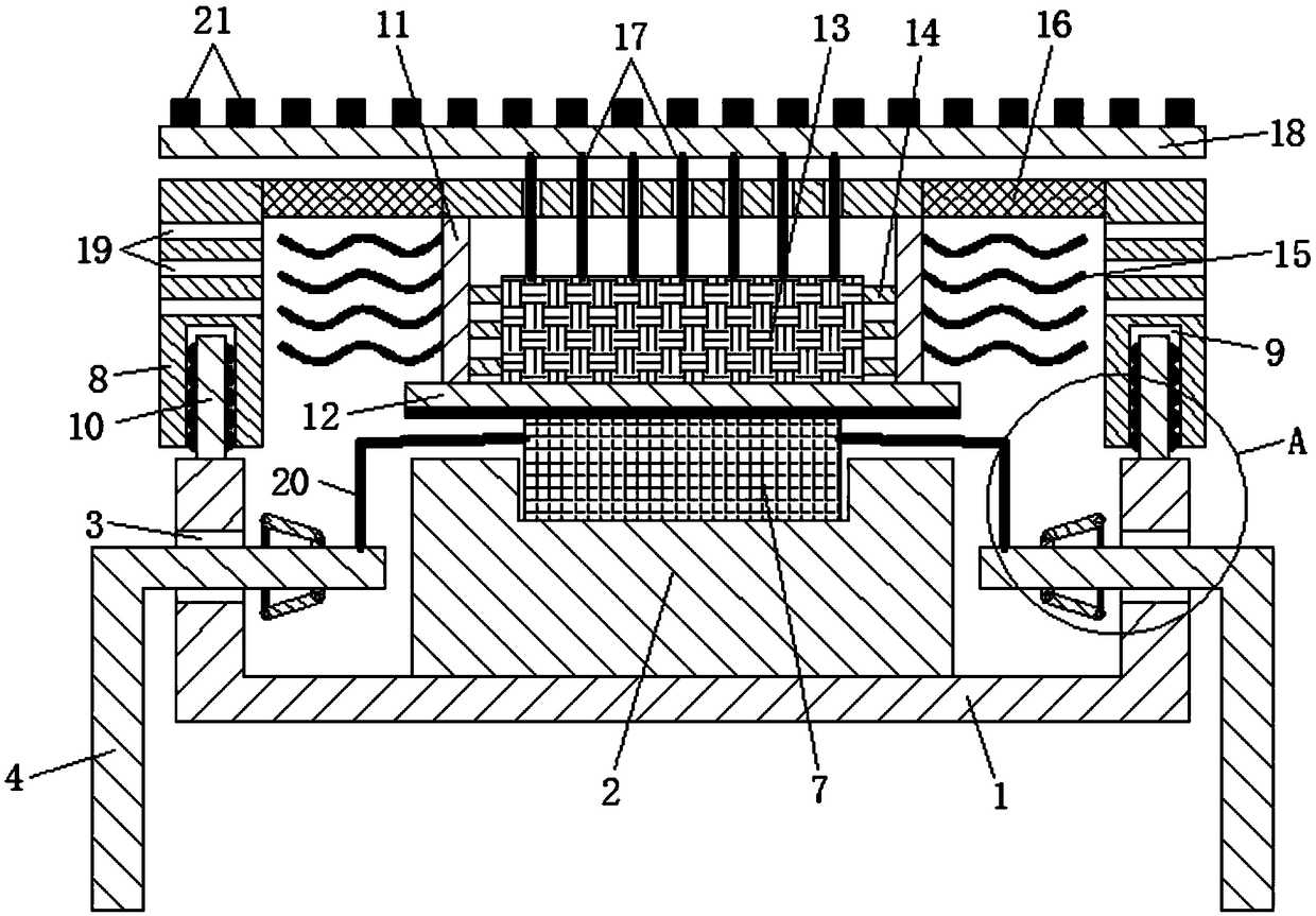
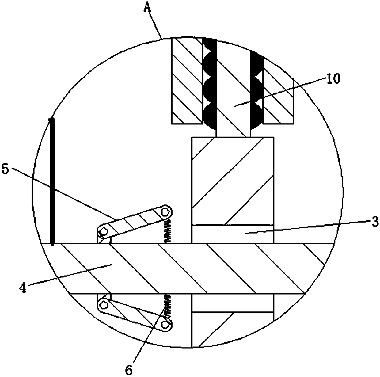
[0023] see Figure 1-2 , the present invention provides a technical solution: a chip packaging structure that is easy to dissipate heat, including a substrate 1, the center of the substrate 1 is fixedly connected with a packaging platform 2, and both sides of the substrate 1 are provided with slots 3, and inside the slots 3 Pin 4 is inserted, one end of pin 4 is movably connected to movable block 5 on both sides, one end of movable block 5 is fixedly connected...


PUM


Abstract

The invention relates to a chip package structure easy to cool and a package method of the chip package structure. The chip package structure comprises a substrate, wherein a package table is fixedlyconnected with a center of the substrate, slots are formed in two sides of the substrate, pins are inserted into the slots, movable blocks are movably connected with two sides of one end of each pin,a spring is fixedly connected with one end of each movable block, a chip body is inserted into a groove in the top of the package table, a package rack is arranged on the chip body, clamping grooves are formed in the bottoms of two sides of the package rack, clamping blocks are fixedly connected with the tops of two sides of the substrate, a heat conduction plate is fixedly connected with the bottom of the package rack, a heat absorption plate is fixedly connected with the bottom of the heat conduction plate, a heat conduction block is fixedly connected with the heat absorption plate, heat conduction rods are fixedly connected with two sides of the heat conduction block, a plurality of cooling fins are fixedly connected to a side wall of the heat conduction plate, dustproof nets are arranged at two sides of the top of the package rack, a plurality of cooling rods are fixedly connected to the top of the heat conduction block, a cooling plate is fixedly connected to a top end of each cooling rod, a plurality of cooling holes are formed in side walls of two sides of the package rack, and wires are electrically connected with two sides of the chip body.

Description

technical field [0001] The invention relates to the technical field of electronic components, in particular to a chip packaging structure that is easy to dissipate heat and a packaging method thereof. Background technique [0002] Chips, also known as microcircuits, microchips, and integrated circuits, refer to silicon chips that contain integrated circuits. They are small in size and are often part of computers or other electronic devices. The chip generally refers to the carrier of the integrated circuit, which is also the result of the design, manufacture, packaging, and testing of the integrated circuit. The integrated circuit is the most important part of electronic equipment, which undertakes the functions of computing and storage. The application range of integrated circuits covers Almost all electronic equipment for military and civilian use. Packaging is the process of assembling integrated circuits into chip final products. Simply put, it is to put the bare integr...

Claims


Application Information

Patent Timeline
Patent Type & Authority Applications(China)
IPC IPC(8): H01L23/31H01L23/367H01L23/467
CPCH01L23/3114H01L23/3672H01L23/467
Inventor 不公告发明人
Owner 常熟市华通电子有限公司
Why Eureka
Try Eureka