Wafer cleaning device

A technology for cleaning devices and wafers, used in electrical components, semiconductor/solid-state device manufacturing, circuits, etc., can solve problems affecting wafer quality, liquid splashing, liquid penetration, etc., to improve user convenience, improve cleanliness, The effect of preventing conduction

Inactive Publication Date: 2019-03-01
HUAIAN IMAGING DEVICE MFGR CORP
View PDF3 Cites 6 Cited by
  • Summary
  • Abstract
  • Description
  • Claims
  • Application Information

AI Technical Summary

Problems solved by technology

[0005] However, in the prior art, the control of granular particles on the front and back of the wafer is better, and the cleaning effect on the particles at the edge of the wafer is poor
Specifically, it is necessary to fix the wafer from the front and make the wafer horizontal, and then spray liquid to the back of the wafer, which may easily lead to failure to clean the fixed point, liquid penetration to the front of the wafer, and serious splashing of liquid in the reaction chamber, etc. Various problems affect the quality of the wafer

Method used


Image

  • Wafer cleaning device
  • Wafer cleaning device
  • Wafer cleaning device

Examples


Embodiment Construction

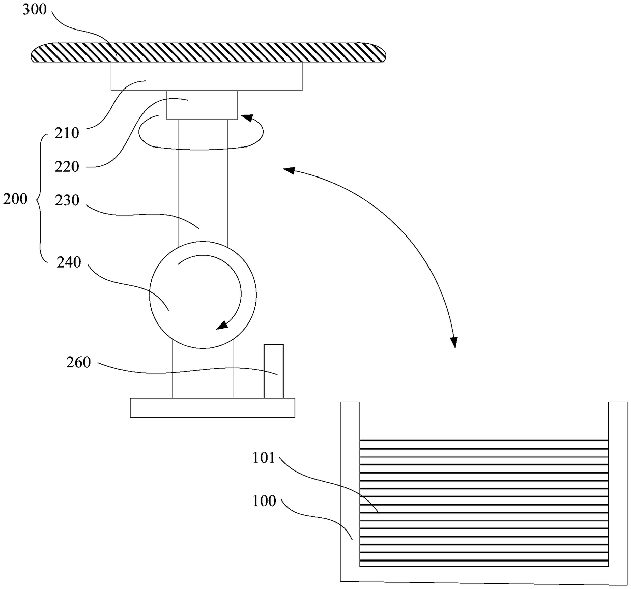
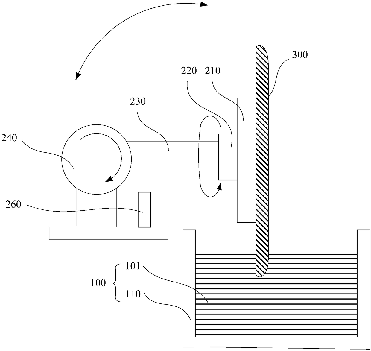
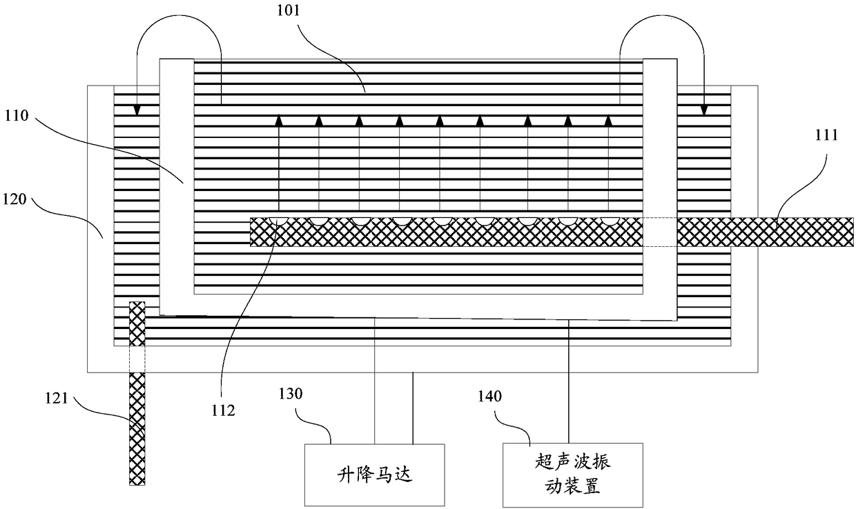
[0027] In the prior art, in the front bonding process of the carrier wafer and the semiconductor substrate, it is required to be tightly bonded and the bonding surface is free of solid particles and air bulges, so it is necessary to improve the front, back and edge of the wafer. cleanliness. However, in the prior art, the particle cleaning effect at the edge of the wafer is poor.

[0028] More specifically, the main factors affecting the cleanliness of the wafer are the film layer at the edge of the wafer and particle defects such as particles, chips, and peeling, followed by particle defects on the surface of the wafer. The granular particles on the front and back of the wafer can be effectively controlled by the existing wafer surface treatment technology. However, the etching of the film layer at the edge of the wafer and the defect treatment cannot achieve accurate etching and effective cleaning in the existing hardware design.

[0029] The inventor of the present invent...


PUM


Abstract

A wafer cleaning device comprises a cleaning groove and wafer fixing equipment, wherein a cleaning liquid is accommodated in the cleaning groove, the wafer fixing equipment is used for grabbing a wafer, the wafer is placed in the cleaning groove in a non-horizontal state, the wafer fixing equipment is used for immersing at least one part of the wafer in the cleaning liquid in a cleaning state anddriving the wafer to rotate. With the wafer cleaning device provided by the scheme, the wafer edge cleaning controllability and cleanness can be improved.

Description

technical field [0001] The invention relates to the field of semiconductor manufacturing equipment, in particular to a wafer cleaning device. Background technique [0002] The image sensor is the core component of the camera equipment, which realizes the image capture function by converting the optical signal into an electrical signal. Taking Complementary Metal Oxide Semiconductor Image Sensors (CMOS Image Sensors, CIS) devices as an example, due to their advantages of low power consumption and high signal-to-noise ratio, they have been widely used in various fields. [0003] Taking Back-side Illumination (BSI) CIS as an example, in the existing manufacturing process, logic devices, pixel devices and metal interconnection structures are first formed in the semiconductor substrate, and then the carrier wafer and the semiconductor The front side of the substrate is bonded, and then the back of the semiconductor substrate is thinned, and the subsequent process of forming a CI...

Claims


Application Information

Patent Timeline
Patent Type & Authority Applications(China)
IPC IPC(8): H01L21/67H01L21/683
CPCH01L21/67057H01L21/6838
Inventor 朱小凡赵黎
Owner HUAIAN IMAGING DEVICE MFGR CORP
Why Eureka
Try Eureka