RGB LED integrated packaging module

A technology of integrated packaging and chips, applied in the direction of electrical components, electric solid devices, circuits, etc., can solve the problems of complex structure and numerous connecting pins, reduce connecting pins, facilitate maintenance and replacement, improve practicability and applicability sexual effect

Pending Publication Date: 2019-03-01
吉安市木林森显示器件有限公司
View PDF7 Cites 2 Cited by
  • Summary
  • Abstract
  • Description
  • Claims
  • Application Information

AI Technical Summary

Problems solved by technology

[0004] The solution of this application is to provide an RGB LED integrated packaging module for the above-mentioned CHIP type LED, TOP type LED, and COB RGB LED integrated modules.

Method used


Image

  • RGB LED integrated packaging module
  • RGB LED integrated packaging module
  • RGB LED integrated packaging module

Examples


Embodiment 1

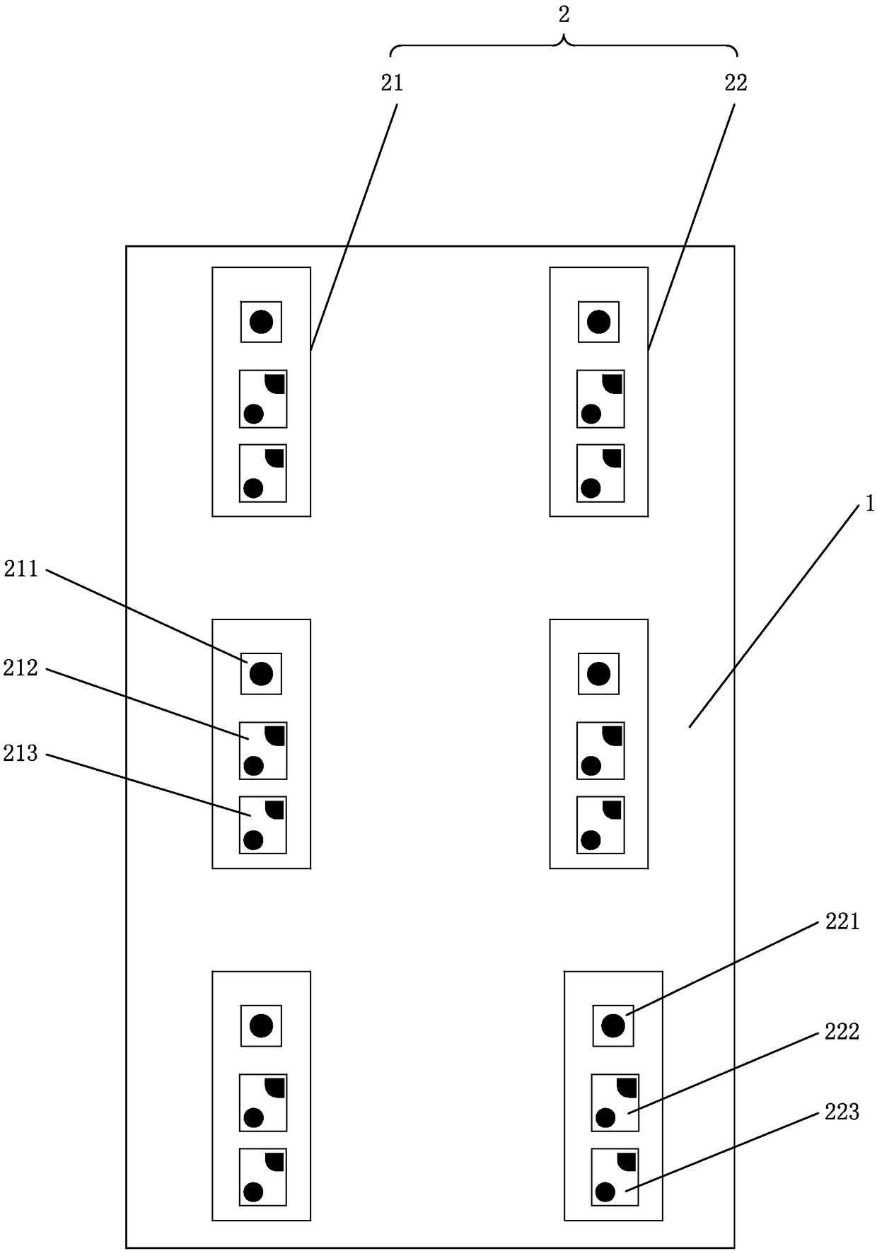
[0058] Such as Figure 1 to Figure 6 As shown, each of the light emitting groups 2 includes a first light emitting unit 21 and a second light emitting unit 22 , and the first light emitting unit 21 includes a first red chip 211 , a first green chip 212 and a first blue chip 213 . The second light emitting unit 22 includes a second red chip 221 , a second green chip 222 and a second blue chip 223 . The first electrode of the first red chip 211 in each of the light-emitting groups 2 is connected in parallel with the first electrode of the first green chip 212 and the first electrode of the first blue chip 213 to form a first Parallel branch, the first electrode of the second red chip 221 in each of the light-emitting groups 2 is connected in parallel with the first electrode of the second green chip 222 and the first electrode of the second blue chip 223 And a second parallel branch is formed, and the second parallel branch is connected in parallel with the first parallel branc...

Embodiment 2

[0069] Embodiment 2, its difference with embodiment 1 is:

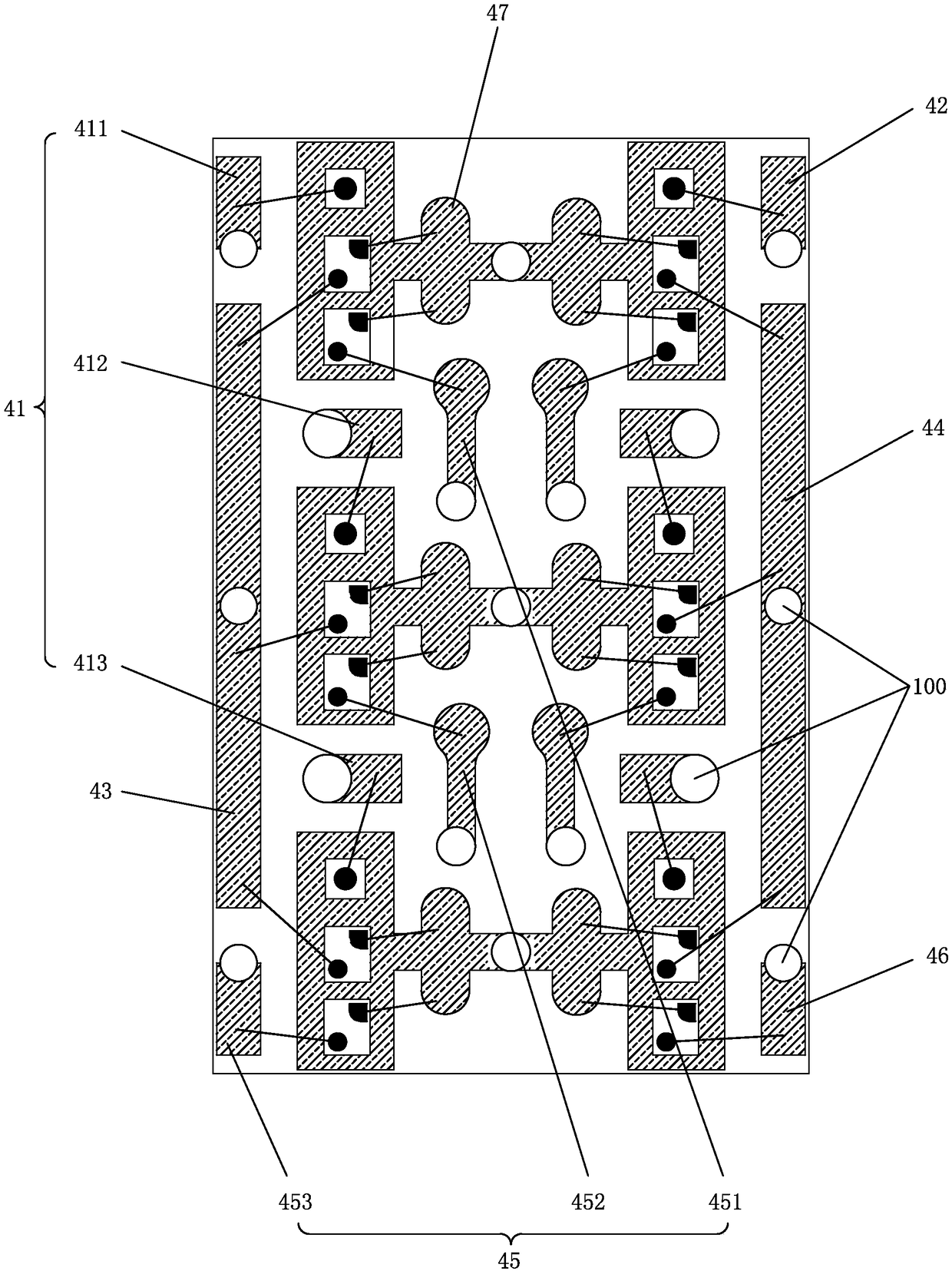
[0070] Such as Figure 7 As shown, the front homopolar region 47 is a common anode region. The first R region 41 is arranged symmetrically with the first two R regions 42 , and it includes the second upper front R region 414 located on the rear side of the first light-emitting unit 21 on the uppermost side, and the first light-emitting region 414 located in the middle. The second middle front R region 415 on the rear side of the unit 21, and the second lower front R region 416 located on the rear side of the first light-emitting unit 21 in the lowermost layer. The previous B zone 45 is arranged symmetrically with the first two B zones 46, and it includes the second upper previous B zone 454 located on the lower right side of the second upper previous R zone 414, and the second upper previous B zone 454 located at the second The second middle front B region 455 on the lower right side of the middle front R region 415...

Embodiment 3

[0071] Embodiment 3, its difference with embodiment 1 is:

[0072] Such as Figure 8 with Figure 9 As shown, the number of the light-emitting groups 2 is 2 groups, which are arranged sequentially from top to bottom, and also include a third light-emitting unit 23 arranged between the first light-emitting unit 21 and the second light-emitting unit 22, The third light emitting unit 23 includes a third red chip 231 , a third green chip 232 and a third blue chip 233 .

[0073] The previous R zone 41 includes a total previous R zone 417 located on the left side of the first light emitting unit 21 on the upper side, a separate previous R zone 418 located on the right side of the first light emitting unit 21 on the upper side, and a separate previous R zone 418 located on the right side of the first light emitting unit 21 on the upper side. The lower part of the first light-emitting unit 21 on the right side is the next R region 419 .

[0074] The previous G zone 43 includes a to...


PUM


Abstract

The invention discloses an RGB LED integrated packaging module, comprising a substrate and at least three groups of light emitting groups arranged on the substrate, wherein each light-emitting group comprises a first light-emitting unit and a second light-emitting unit; the first light emitting unit comprises a first red wafer, a first green wafer and a first blue wafer. The second light emittingunit comprises a second red wafer, a second green wafer and a second blue wafer. Six light emitting units in the three groups of light emitting units are integrated, and then the six independent light-emitting units are combined into an LED integration module, and meanwhile, the first red wafer, the first green wafer, the first blue wafer, the second red wafer, the second green wafer and the second blue wafer in the same group are connected in parallel through a common negative circuit or a common positive circuit, and then are connected with the first same-color wafers and the second same-color wafers between the groups, so that the connection pins can be reduced to the maximum extent and the tin loading area can be reduced, and the SMT chip mounting efficiency can be improved; and meanwhile, the packaging structure is simplified.

Description

【Technical field】 [0001] The technical field of LED optoelectronic device manufacturing in this application specifically relates to an RGB LED integrated packaging module. 【Background technique】 [0002] In recent years, in the indoor large-screen display market, small-pitch LED displays have grown rapidly, with a market share of nearly 40%. [0003] At present, there are three main solutions for small-pitch LED displays: small-size CHIP-type LED placement, small-size TOP-type LED placement, and COB RGB assembly. In terms of accuracy and SMT efficiency, it is difficult to achieve satisfactory results. As for the small-pitch LED display assembled by the third COB RGB packaging method, there have always been problems such as board color difference, board warpage, and low process yield. The technical problems to be solved, and the three types of LED integrated modules still have technical problems such as complex structure and numerous connecting pins, which makes the existing...

Claims


Application Information

Patent Timeline
Patent Type & Authority Applications(China)
IPC IPC(8): H01L25/075H01L33/54H01L33/56H01L33/62
CPCH01L25/0753H01L33/54H01L33/56H01L33/62
Inventor 张盛彭昕
Owner 吉安市木林森显示器件有限公司
Why Eureka
Try Eureka