

Display device and manufacturing method thereof
A display device and display panel technology, which is applied in the recognition device, the photoengraving process of the pattern surface, optics and other directions, can solve the problems of high power consumption and reduce the utilization rate of light energy, so as to reduce the power consumption and improve the utilization rate. , observe the effect of narrowing the viewing angle
- Summary
- Abstract
- Description
- Claims
- Application Information
AI Technical Summary
Problems solved by technology
Method used
Image

Examples
Embodiment 1
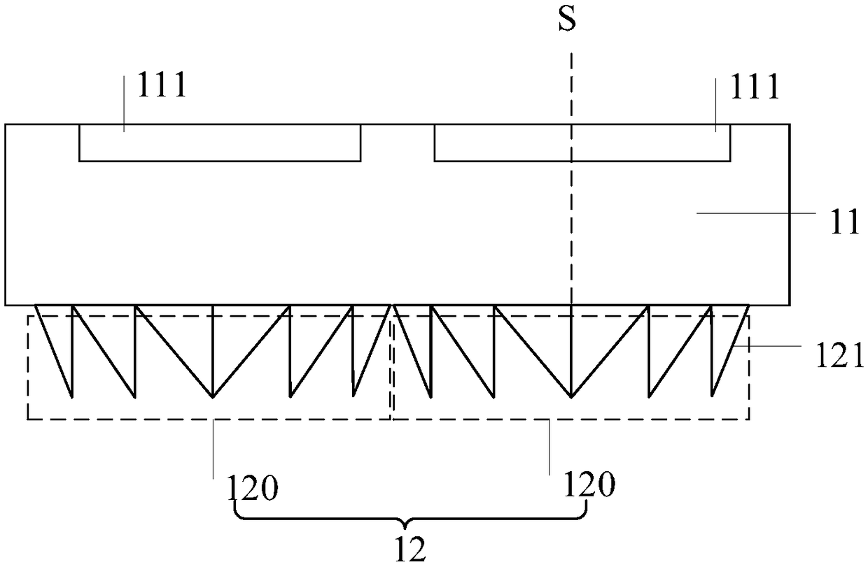
[0035] refer to figure 1 , shows a schematic structural diagram of a display device according to an embodiment of the present invention.
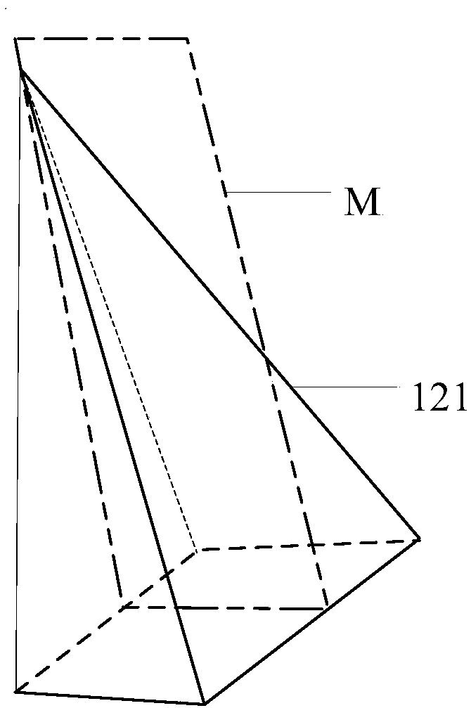
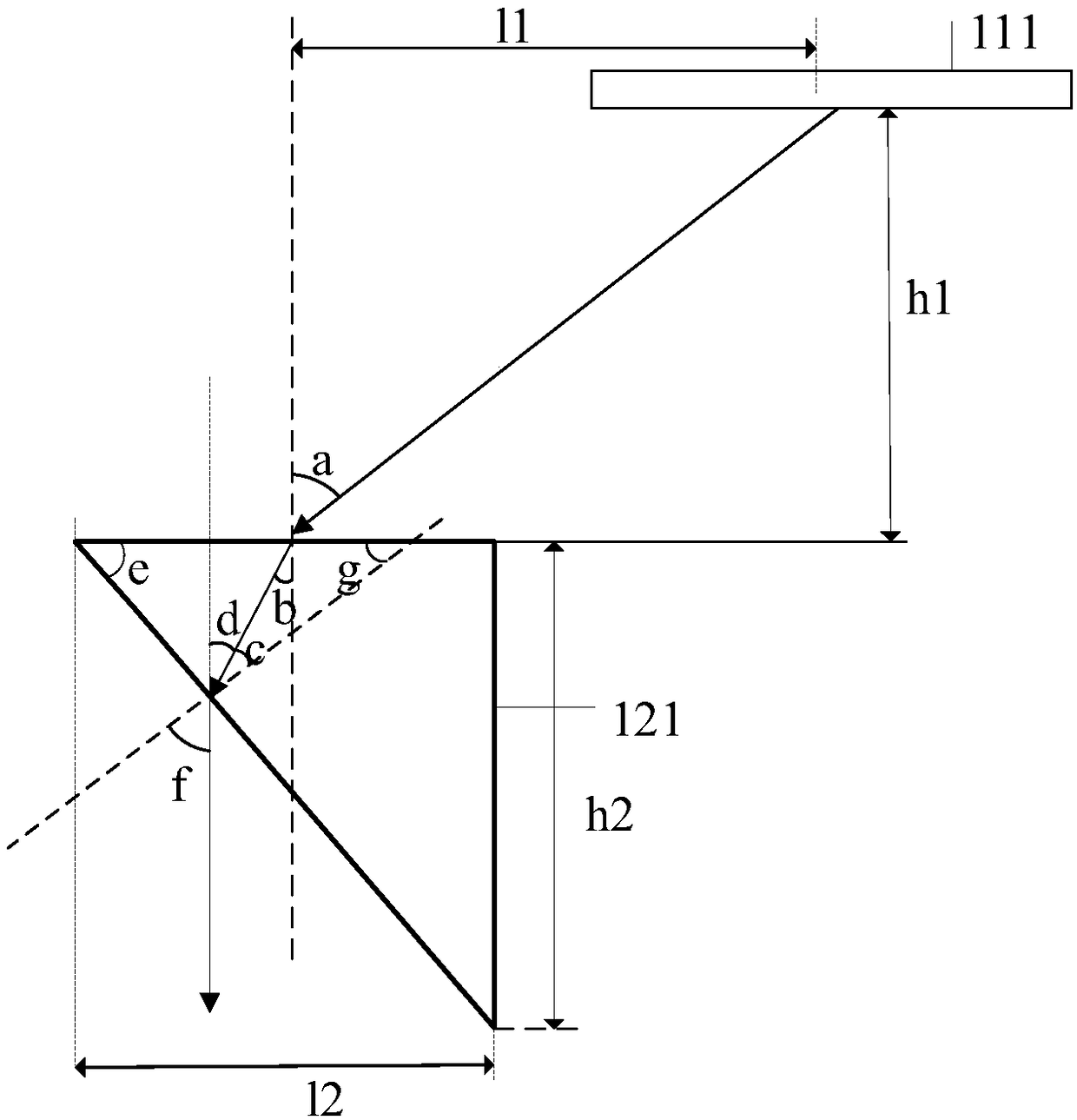
[0036] An embodiment of the present invention provides a display device, including a display panel 11 and an optical modulation assembly 12 arranged on the light-emitting side of the display panel 11. The display panel 11 includes a plurality of pixel units 111, and the optical modulation assembly 12 includes a pixel unit 111 one by one. Corresponding to the optical modulation units 120, each optical modulation unit 120 includes a plurality of prisms 121; the prisms 121 are configured to refract the light emitted by the pixel unit 111, so that the refracted light exits at a preset angle.
[0037] A plurality of pixel units 111 are arranged in the display panel 11 for emitting light of corresponding colors so that the user can see the displayed information in the display panel 11. Generally, the light emitted by the pixel units 111 includes ...
Embodiment 2
[0084] refer to Figure 4 , which shows a flow chart of a method for manufacturing a display device according to an embodiment of the present invention, which may specifically include the following steps:
[0085] In step 401, a display panel is provided, and the display panel includes a plurality of pixel units.
[0086] In the embodiment of the present invention, when forming a display device, firstly, a display panel 11 needs to be produced. The display panel 11 can be an LCD display panel or an OLED display panel, and the display panel 11 includes a plurality of pixel units 111, and the plurality of pixel units 111 may be arranged in an array.
[0087]Step 402, forming an optical modulation assembly on the light output side of the display panel, the optical modulation assembly includes optical modulation units corresponding to the pixel units one by one, and each of the optical modulation units includes a plurality of prisms to The light emitted by the pixel unit is refr...
PUM
| Property | Measurement | Unit |
|---|---|---|
| Vertical height | aaaaa | aaaaa |
Abstract
Description
Claims
Application Information