PCB board for camera module

A technology of PCB board and camera module, which is applied to printed circuits connected with non-printed electrical components, printed circuit components, printed circuit stress/deformation reduction, etc., can solve the problem of reducing the variation degree of photosensitive sensors, etc., to achieve The effect of reducing the degree of variation and reducing the change in resolution

Pending Publication Date: 2019-03-12
TRULY OPTO ELECTRONICS
View PDF0 Cites 4 Cited by
  • Summary
  • Abstract
  • Description
  • Claims
  • Application Information

AI Technical Summary

Problems solved by technology

[0003] The technical problem to be solved by the present invention is to provide a PCB board for a camera module, since the reinforcement board is arranged on the upper surface of the multilayer circuit board, and the photosensitive sensor is arranged on the upper surface of the reinforcement board, so that the The strength of the reinforcing plate is stronger than that of other layers. When the PCB board deforms, it will deform in the direction of the layers with lower strength. Therefore, the PCB board will deform downward under high temperature and high humidity environment, which inhibits the PCB board from going down. The upper deformation greatly reduces the variation degree of the photosensitive sensor relative to the lens, so that without changing the grounding performance, the resolution of the camera module changes little, and clear photos can still be taken

Method used


Image

  • PCB board for camera module
  • PCB board for camera module
  • PCB board for camera module

Examples


Embodiment Construction

[0024] The present invention will be described in detail below in conjunction with examples, which are only preferred implementations of the present invention, and are not limitations of the present invention.

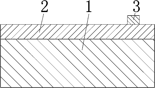
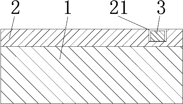
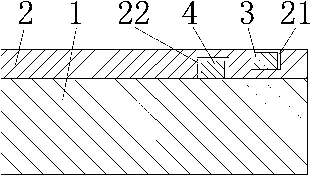
[0025] see figure 1 , is a kind of PCB board that is used for camera module provided by the present invention, and it comprises multilayer circuit board 1, reinforcement board 2 and photosensitive sensor 3, multilayer circuit board 1 usually comprises base layer, and copper layer is arranged on both sides of base layer, The outer side of the copper layer is covered with an insulating layer; the reinforcing board 2 is arranged on the upper surface of the multilayer circuit board 1; It is transformed into an electrical signal for reception by the camera module. Since the reinforcement board 2 is arranged on the upper surface of the multilayer circuit board 1, and the photosensitive sensor 3 is arranged on the upper surface of the reinforcement board 2, the strength near...


PUM


Abstract

The invention discloses a PCB board for a camera module. The PCB board comprises a multi-layer circuit board, a reinforcing board and a photosensitive sensor. The reinforcing board is arranged on theupper surface of the multi-layer circuit board; and the photosensitive sensor is arranged on the upper surface of the reinforcing board. The reinforcing board is arranged on the upper surface of the multi-layer circuit board and the photosensitive sensor is arranged on the upper surface of the reinforcing board so that the strength near the reinforcing board is stronger than that of other layers;during deformation, the PCB board is deformed towards the direction of the layers with low strength; therefore, the PCB board is downward deformed in a high-temperature and high-humidity environment,thereby prohibiting the PCB board from being upward deformed; the variation degree of the photosensitive sensor relative to a lens is greatly reduced; in the case of not changing the grounding performance, the resolving power of the camera module changes little; and shooting of clear pictures can still be ensured.

Description

technical field [0001] The invention relates to the technical field of printed circuit boards, and more specifically, relates to a PCB board used for a camera module. Background technique [0002] The current front cameras of mobile phones are all fixed-focus models, and major mobile phone manufacturers are trying to upgrade the pixels of the front cameras. 20M / 24M / 25M has become the mainstream configuration today, and the flagship models will be upgraded to 36M in the next stage. / 48M, with the pixel upgrade, the requirements for each material are getting higher and higher, and the requirements for the variation of materials are also getting higher and higher. The bottom plate of the existing camera is a multi-layer PCB board, and a photosensitive sensor is arranged on the top of the PCB board. Because the materials between the layers are different, the moisture absorption and thermal expansion coefficients of the materials are also different, resulting in the PCB board pas...

Claims


Application Information

Patent Timeline
Patent Type & Authority Applications(China)
IPC IPC(8): H05K1/02H05K1/18
CPCH05K1/0271H05K1/18
Inventor 刘自红姚波
Owner TRULY OPTO ELECTRONICS
Why Eureka
Try Eureka