Silicon Etching Solution and Method for Producing Silicon Device Using the Etching Solution
a technology of silicon etching solution and etching solution, which is applied in the direction of crystal growth process, after-treatment details, polycrystalline material growth, etc., can solve the problems of high accuracy and inability to selective etching of polysilicon films, and achieves small etching rate, small etching rate, and reduced etching rate.
- Summary
- Abstract
- Description
- Claims
- Application Information
AI Technical Summary
Benefits of technology
Problems solved by technology
Method used
Image
Examples
example 1
[0109]As the silicon etching solution, a silicon etching solution having a composition shown in Table 1 was prepared using propylene glycol monopropyl ether as the compound represented by the formula (1).
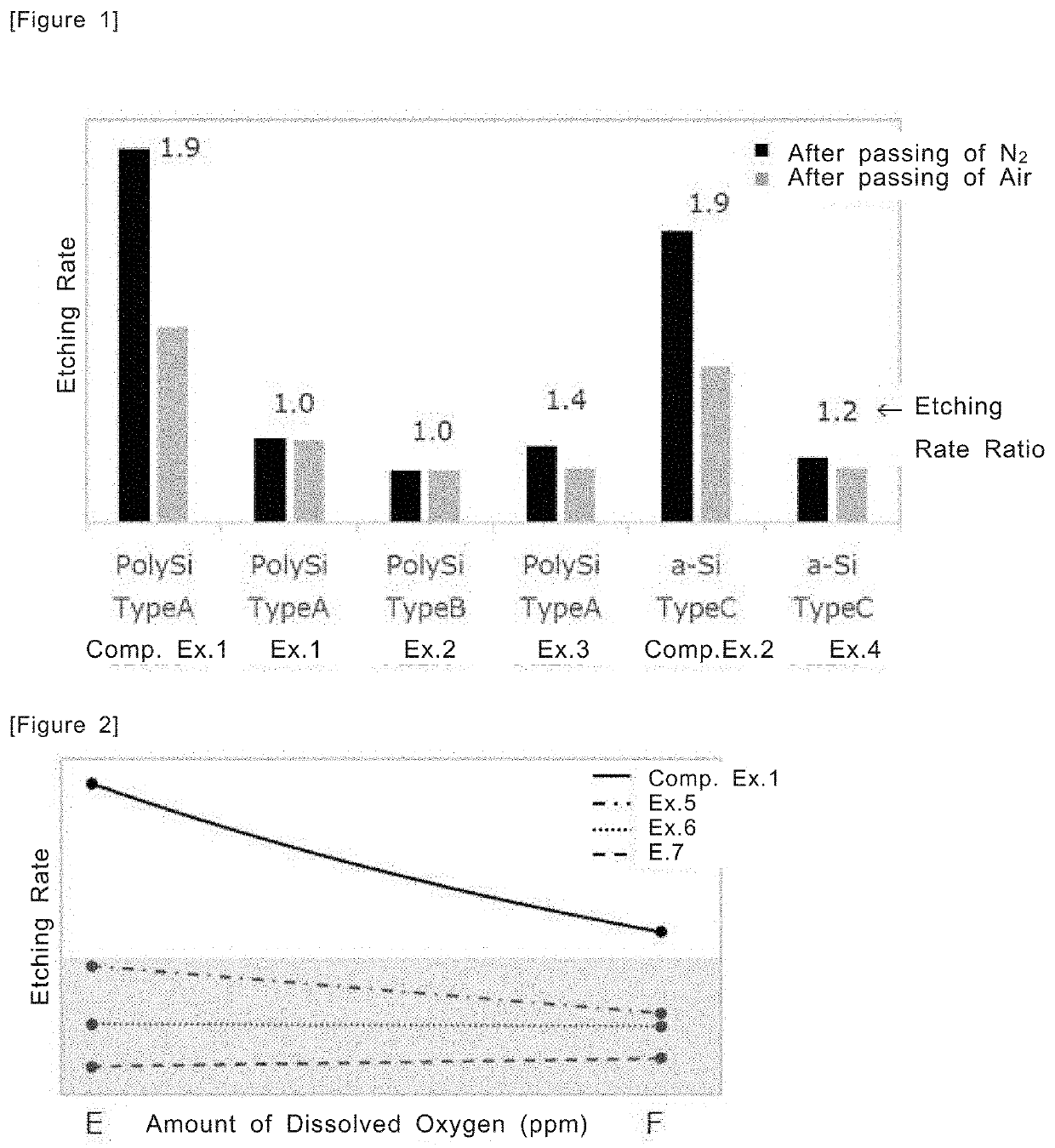
[0110]Using the silicon etching solution prepared, a ratio (RN / RA) of an etching rate (RN) after passing of N2 at a solution temperature of 40° C. to an etching rate (RA) after passing of air at the same solution temperature was measured assuming etching at a solution temperature of 40° C. In each of the examples and the comparative examples, the dissolved oxygen concentration of the silicon etching solution after passing of N2 was 1 ppm or less, and the saturated dissolved oxygen concentration thereof after passing of air was 4 ppm or less.
[0111]For determining the etching rate (RN) after passing of N2, into the silicon etching solution having been heated to a solution temperature of 40° C., N2 gas was passed by bubbling until the dissolved oxygen concentration decreased to a const...
example 2
[0112]An etching rate ratio (RN / RA) was calculated in the same manner as in Example 1, except that a silicon etching solution having a composition shown in Table 1 was used as the silicon etching solution, and a polysilicon substrate (PolySi TypeB) obtained by polysilicon film formation was used as the object silicon substrate. The PolySi TypeA and the PolySi TypeB have films different from each other in the film thickness or obtained by different film forming conditions such as annealing conditions. The result is shown in Table 1 and FIG. 1.
example 3
[0113]An etching rate ratio (RN / RA) was calculated in the same manner as in Example 1, except that a silicon etching solution having a composition shown in Table 1 was used as the silicon etching solution. The result is shown in Table 1 and FIG. 1.
PUM
| Property | Measurement | Unit |
|---|---|---|
| concentration | aaaaa | aaaaa |
| charge storage | aaaaa | aaaaa |
| volumes | aaaaa | aaaaa |
Abstract
Description
Claims
Application Information


