All-inorganic LED lamp and packaging method thereof
A technology of LED lamps and packaging methods, which is applied in the direction of electrical components, circuits, semiconductor devices, etc., and can solve problems such as the inappropriateness of ultraviolet LED chips
- Summary
- Abstract
- Description
- Claims
- Application Information
AI Technical Summary
Problems solved by technology
Method used
Image
Examples
Embodiment 1
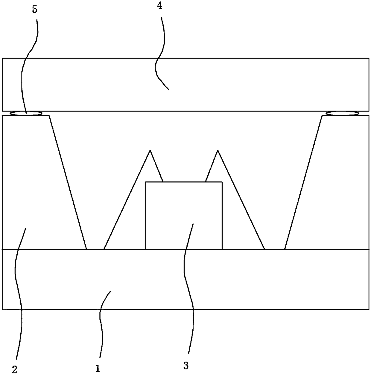
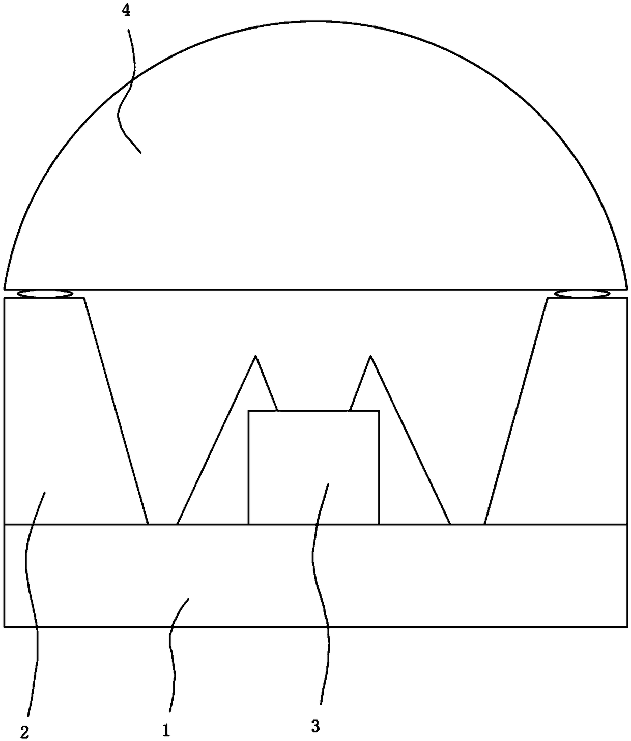
[0025] like figure 1 and figure 2 As shown, an all-inorganic LED lamp includes a base 1, a groove is opened on the base 1 to form a bowl 2 or a dam provided on the base 1 forms a bowl 2, and the bowl 2 is provided with an ultraviolet The LED chip 3 and the ultraviolet LED chip 3 are electrically connected to the base 1 .
[0026] The glass cover plate 4 is a monolithic glass structure, a glass cover plate provided with a metal layer or a glass cover plate provided with a metal frame, and the glass in the glass cover plate 4 is a monolithic planar hard glass or a glass lens, and the glass lens is opposite to the The laser has a focused effect and is suitable for directional applications.
[0027] The surface of the bowl 2 is coated with solder 5 with a thickness of 0.02-0.5 mm. In this embodiment, the solder is metal solder, metal and inorganic mixed solder or sintered silver glue. Under vacuum or inert gas, the glass cover plate 4 Place it on the solder 5 on the bowl cup 2...
Embodiment 2
[0029] like figure 1 and figure 2 As shown, an all-inorganic LED lamp includes a base 1, a groove is opened on the base 1 to form a bowl 2 or a dam provided on the base 1 forms a bowl 2, and the bowl 2 is provided with an ultraviolet The LED chip 3 and the ultraviolet LED chip 3 are electrically connected to the base 1 .
[0030]The glass cover plate 4 is a glass cover plate provided with a metal layer or a glass cover plate provided with a metal frame, and the surface of the bowl cup 2 is coated with a solder 5 with a thickness of 0.02-0.5 mm. In this embodiment, the solder is selected from metal solder, Metal and inorganic mixed solder or sintered silver glue, under vacuum or inert gas, place the glass cover 4 on the solder 5 on the bowl cup 2, and weld one or more pre-soldered spots on the glass cover 4 with laser , the pre-soldering spots are evenly distributed around the glass cover plate 4 and symmetrically distributed relative to the glass cover plate 4, the glass co...
Embodiment 3
[0032] like figure 1 and figure 2 As shown, the present invention also provides a method for encapsulating an all-inorganic LED lamp, comprising the following steps:
[0033] S1. Pretreatment: including preparing the base 1 with the bowl cup 2 and the ultraviolet LED chip 3; preparing the glass cover 4, the glass cover 4 is a whole glass structure, a glass cover with a metal layer or a metal The glass cover plate of the frame, and the glass in the glass cover plate 4 is a whole piece of flat hard glass or glass lens, and the glass lens has a gathering effect on the laser light, which is suitable for directional applications;
[0034] S2, fixing the ultraviolet LED chip 3 in the bowl cup 2;
[0035] S3, coating the solder 5 on the surface of the bowl cup 2, the coating thickness of the solder 5 is 0.02-0.5 mm;
[0036] S4. In a vacuum or an inert gas environment, vacuumize the vacuum environment, and the inert gas can be nitrogen, etc., and place the glass cover plate 4 on ...
PUM
| Property | Measurement | Unit |
|---|---|---|
| Thickness | aaaaa | aaaaa |
Abstract
Description
Claims
Application Information

