Ceramic package housing

A ceramic packaging and housing technology, applied in the direction of electrical components, electrical solid devices, circuits, etc., can solve the problems of miniaturization of the outer dimensions of the housing, meet the development trend of miniaturization design, reduce the overall size, and ensure brazing The effect of intensity

Inactive Publication Date: 2019-03-19
THE 13TH RES INST OF CHINA ELECTRONICS TECH GRP CORP
View PDF5 Cites 5 Cited by
  • Summary
  • Abstract
  • Description
  • Claims
  • Application Information

AI Technical Summary

Problems solved by technology

This method requires that the length of the welding pad between the lead wire and the shell is more than 1.0mm, and in order to ensure reliability, it is generally required that the distance between the pad and the edge of the outer shape is more than 0.05mm, and the further miniaturization of the outer dimension of the outer shell cannot be achieved.

Method used


Image

  • Ceramic package housing
  • Ceramic package housing
  • Ceramic package housing

Examples


Embodiment Construction

[0025] In order to make the technical problems, technical solutions and beneficial effects to be solved by the present invention clearer, the present invention will be further described in detail below in conjunction with the accompanying drawings and embodiments. It should be understood that the specific embodiments described here are only used to explain the present invention, not to limit the present invention.

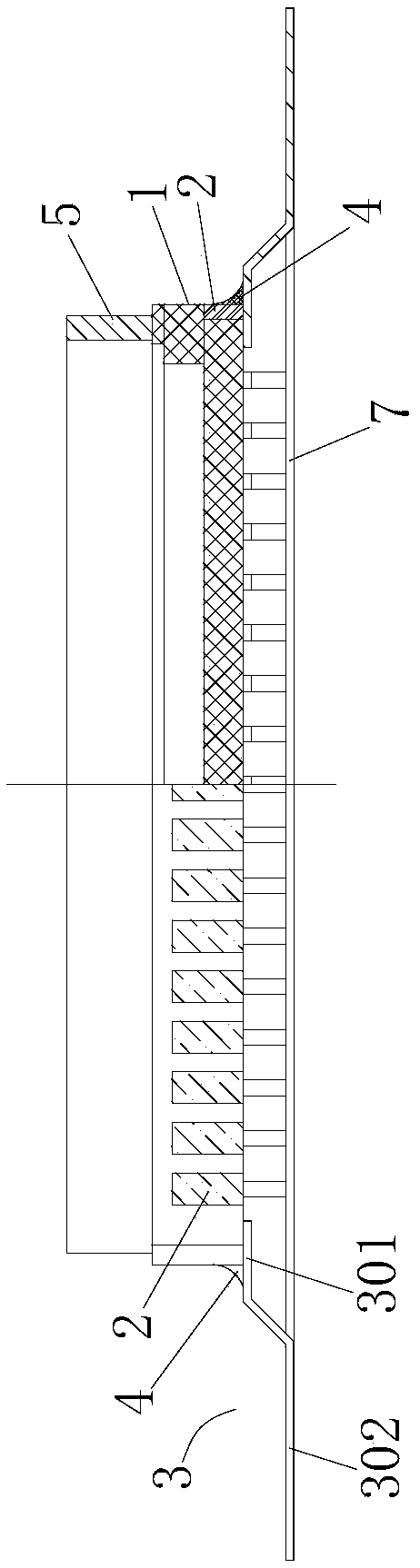
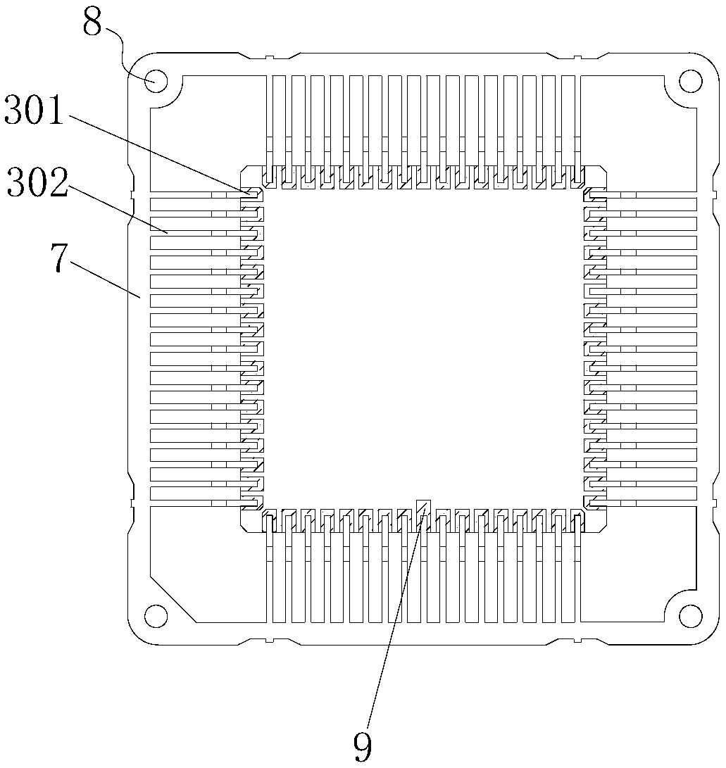
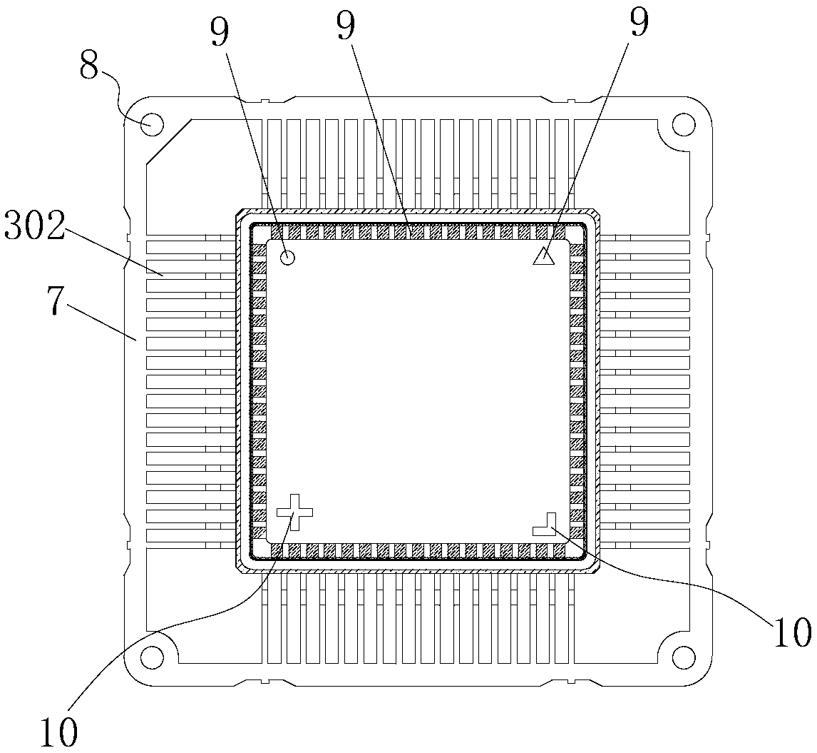
[0026] Please also refer to Figure 1 to Figure 6 , the ceramic packaging shell provided by the present invention will now be described. The ceramic package shell includes a ceramic part 1, a pad 2 arranged on the outer peripheral side of the ceramic part 1, and a lead wire 3 arranged at the bottom of the ceramic part 1 and extending toward the outer periphery of the ceramic part 1; the pad 2 corresponds to the lead wire 3 one by one , the pad 2 is welded to the lead 3 , and the welding wrap 4 is located outside the pad 2 .

[0027] In the ceramic package shell p...


PUM

PropertyMeasurementUnit
widthaaaaaaaaaa
heightaaaaaaaaaa
widthaaaaaaaaaa

Abstract

The present invention provides a ceramic package housing and belongs to the field of ceramic packaging. The ceramic package housing comprises a ceramic component, pads disposed on the outer peripheralside of the ceramic component, and leads which are disposed at the bottom of the ceramic component and extend toward the periphery of the ceramic component; the pads are in one-to-one correspondencewith the leads; the pads are soldered to the leads; and solder wrap angles are located at the outer sides the pads. According to the ceramic package housing provided by the invention, the pads are disposed at the outer peripheral side of the ceramic component; the leads are soldered to the outer sides of the pads, so that the solder wrap angles are formed, and therefore, the reinforcement of the leads can be realized, the brazing strength of the housing and the leads is ensured, and the soldering reliability of the leads is realized; the size of the pads can be set to be below 0.8mm, and can be as small as 0.2mm at most; and no intervals are required to be left between the pads and the edge of the ceramic component, so that the outer dimension of the housing is reduced by more than 0.5mm,and therefore, the overall size of the ceramic package housing is effectively reduced, and the trend of the miniaturization of the housing can be met.

Description

technical field [0001] The invention belongs to the technical field of ceramic packaging, and more specifically relates to a ceramic packaging shell. Background technique [0002] The traditional CQFP (Ceramic Quad Flat Pack) housing is a four-side pin flat package with a guard ring. This type of housing forms a good "meniscus" solder wrap angle at the front and rear ends of the lead by bending the lead to form a three-dimensional brazing structure, which relieves the impact of external forces on the metallization layer and ensures the welding strength of the lead. reliability. This method requires that the length of the welding pad between the lead wire and the shell is more than 1.0mm, and in order to ensure reliability, the distance between the pad and the edge of the outer shape is generally required to be more than 0.05mm, which cannot achieve further miniaturization of the outer shape of the outer shell. Contents of the invention [0003] The purpose of the present...

Claims


Application Information

Patent Timeline
Patent Type & Authority Applications(China)
IPC IPC(8): H01L23/055H01L23/10
CPCH01L23/055H01L23/10
Inventor 杨振涛
Owner THE 13TH RES INST OF CHINA ELECTRONICS TECH GRP CORP
Why Eureka
Try Eureka