Half bridge package structure

A technology of packaging structure and plastic body, applied in the direction of semiconductor devices, semiconductor/solid-state device parts, electrical components, etc., can solve the problems of unfavorable product miniaturization, large package size, etc., to save external heat sinks, electrical conductivity and thermal conductivity Good performance and reduced thermal resistance

Pending Publication Date: 2019-03-19
SHANDONG JINGDAO MICROELECTRONICS
View PDF12 Cites 0 Cited by
  • Summary
  • Abstract
  • Description
  • Claims
  • Application Information

AI Technical Summary

Problems solved by technology

Although the surface mount technology of electronic components has become a development trend at home and abroad, due to the limitations of certain technologies, high-power components are basically plug-in packages, such as: KBJ, GBU and GBJ, etc., the package size is large, Not conducive to product miniaturization

Method used


Image

  • Half bridge package structure
  • Half bridge package structure
  • Half bridge package structure

Examples


Embodiment Construction

[0023] In order to make the object, technical solution and advantages of the present invention clearer, the present invention will be further described in detail below in conjunction with the accompanying drawings and embodiments. It should be understood that the specific embodiments described here are only used to explain the present invention, not to limit the present invention.

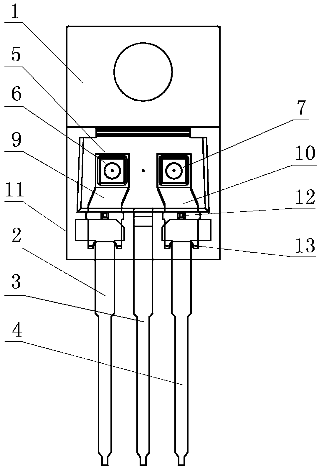
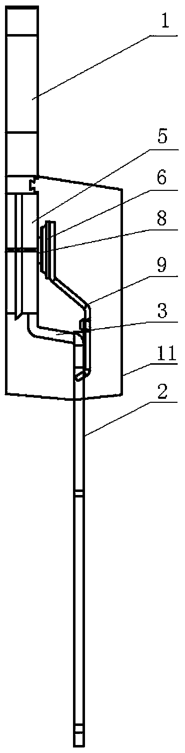
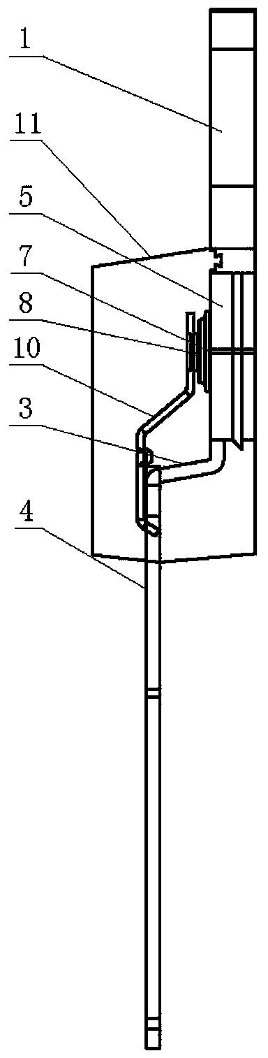
[0024] Such as Figure 1-Figure 3 As shown, the present invention provides a half-bridge packaging structure, including a lead frame 1, a first pin 2, a second pin 3, a third pin 4, a first diode chip 6, a second diode Chip 7, copper grain 8, first jumper 9, second jumper 10, black colloid, plastic package 11, each lead frame 1 corresponds to a first pin 2 and a third pin 4, lead frame 1 It is a separate structure from the first pin 2 and the third pin 4, and each lead frame 1 is provided with two base islands 5 and a second pin 3 drawn out from the lead frame 1, the second pin 3 is arranged betw...


PUM


Abstract

The invention provides a half bridge package structure, belonging to the field of semiconductor component packaging. The half bridge package structure comprises lead frames, a first pin, second pins,a third pin, first diode chips and second diode chips, copper particles, a first jumper, a second jumper, a black colloid and a plastic body. Each lead frame is provided with two base islands and onesecond pin led by the lead frame, the two base islands are respectively provided with one first diode chip and one second diode chip, the P surface of each first diode chip is connected to the islandthrough the copper particles, and the N surface of the first diode chip is connected to the first pin through the first jumper, the N side of the second diode chip is disposed on the base island, andthe P surface of the second diode chip is connected to the third pin through the second jumper; two half bridges can be packaged to form a complete rectifier bridge to replace an in-line bridge package, the structure is simple, and the package can follow the original frame structure which is beneficial to reduce the cost.

Description

technical field [0001] The invention relates to the technical field of packaging of semiconductor components, in particular to a half-bridge packaging structure. Background technique [0002] Since the beginning of the 21st century, China's electronic information product manufacturing industry has grown rapidly at a rate of more than 20% every year. Its scale has ranked second in the world since 2004, and its industrial income has jumped to the first in the world in 2012. Driven by the rapid development of China's electronic information industry, semiconductor rectifier devices have also developed rapidly. With the advancement of science and technology, electronic products are also constantly developing, and electronic products are developing towards light, small and thin. Although the surface mount technology of electronic components has become a development trend at home and abroad, due to the limitations of certain technologies, high-power components are basically plug-i...

Claims


Application Information

Patent Timeline
Patent Type & Authority Applications(China)
IPC IPC(8): H01L23/495H01L25/07
CPCH01L25/072H01L23/49503H01L23/4952H01L2924/181H01L2224/40245H01L2924/00012
Inventor 孔凡伟段花山王福龙
Owner SHANDONG JINGDAO MICROELECTRONICS
Why Eureka
Try Eureka