

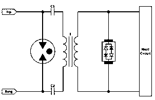
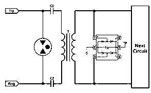
Low capacitance discharge tube array used for G.fast
A discharge tube and low-capacity technology, which is applied in the direction of circuits, electrical components, and electric solid devices, can solve the problems that TVS devices cannot meet the requirements of G•fast applications, and achieve the effects of reducing residual voltage, high production efficiency, and time-consuming
- Summary
- Abstract
- Description
- Claims
- Application Information
AI Technical Summary
Problems solved by technology
Method used
Image

Examples
Embodiment 1
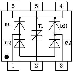
[0032] Example 1, such as Figure 4 As shown, a low-capacity discharge tube array for G•fast includes a first lead 1, a second lead 2, a third lead 3, a fourth lead 4, a fifth lead 5, a sixth lead 6, a first low Capacitance diode chip 7, second low-capacity diode chip 8, third low-capacity diode chip 9, fourth low-capacity diode chip 10, discharge tube chip 11 and plastic package 12;
[0033] The first lead 1, the second lead 2, and the third lead 3 share the first patch base island 1-1, and the fourth lead 4, the fifth lead 5, and the sixth lead 6 have the second patch base island 2-1 respectively. , the third patch base island 3-1 and the fourth patch base island 4-1;
[0034] The back of the first low-capacity diode chip 7, the second low-capacity diode chip 8, the third low-capacity diode chip 9 and the fourth low-capacity diode chip 10 is a cathode, and the surface is an anode;
[0035] The cathode of the first low-capacity diode chip 7 is welded to the common first pat...
Embodiment 2
[0044] Example 2, such as Figure 5 , a low-capacity discharge tube array for G•fast, including a first lead 1, a second lead 2, a third lead 3, a fourth lead 4, a fifth lead 5, a sixth lead 6, a first low-capacity diode Chip 7, second low-capacity diode chip 8, third low-capacity diode chip 9, fourth low-capacity diode chip 10, discharge tube chip 11 and plastic package 12;
[0045] The first lead 1, the second lead 2, and the third lead 3 share the first patch base island 1-1, and the fourth lead 4, the fifth lead 5, and the sixth lead 6 have the second patch base island 2-1 respectively. , the third patch base island 3-1 and the fourth patch base island 4-1;
[0046] The back side of the first low-capacity diode chip 7, the second low-capacity diode chip 8, the third low-capacity diode chip 9 and the fourth low-capacity diode chip 10 is an anode, and the surface is a cathode;
[0047] The anode of the first low-capacity diode chip 7 is welded to the second patch base isla...
Embodiment 3
[0053] Example 3, such as Figure 6 , a low-capacity discharge tube array for G•fast, including a first lead 1, a second lead 2, a third lead 3, a fourth lead 4, a fifth lead 5, a sixth lead 6, a first low-capacity diode Chip 7, second low-capacity diode chip 8, third low-capacity diode chip 9, fourth low-capacity diode chip 10, discharge tube chip 11 and plastic package 12;
[0054] The first lead 1, the second lead 2, and the third lead 3 share the first patch base island 1-1, and the fourth lead 4, the fifth lead 5, and the sixth lead 6 have the second patch base island 2-1 respectively. , the third patch base island 3-1 and the fourth patch base island 4-1;
[0055] The back side of the first low-capacity diode chip 7 and the second low-capacity diode chip 8 are cathodes, and the front side is an anode;
[0056] The back of the third low-capacity diode chip 9 and the fourth low-capacity diode chip 10 are anodes, and the surfaces are cathodes;
[0057] The cathode of the...
PUM
 Abstract
Description
Claims
Application Information