Liquid crystal display panel and liquid crystal display device

A liquid crystal display panel, liquid crystal layer technology, applied in nonlinear optics, instruments, optics, etc., can solve the problems of slow liquid crystal response speed, image display stuck, affecting display quality, etc., to increase transmittance and reduce response time. , Improve the effect of screen display quality

Pending Publication Date: 2019-03-26
KUSN INFOVISION OPTOELECTRONICS
View PDF8 Cites 2 Cited by
  • Summary
  • Abstract
  • Description
  • Claims
  • Application Information

AI Technical Summary

Problems solved by technology

[0005] In order to overcome the shortcomings and deficiencies existing in the prior art, the purpose of the present invention is to provide a liquid crystal display panel and a liquid crystal display device to solve the slow response speed and long response time of liquid crystals in the prior art, resulting in freezes when displaying images. Problems affecting display quality

Method used


Image

  • Liquid crystal display panel and liquid crystal display device
  • Liquid crystal display panel and liquid crystal display device
  • Liquid crystal display panel and liquid crystal display device

Examples


Embodiment 1

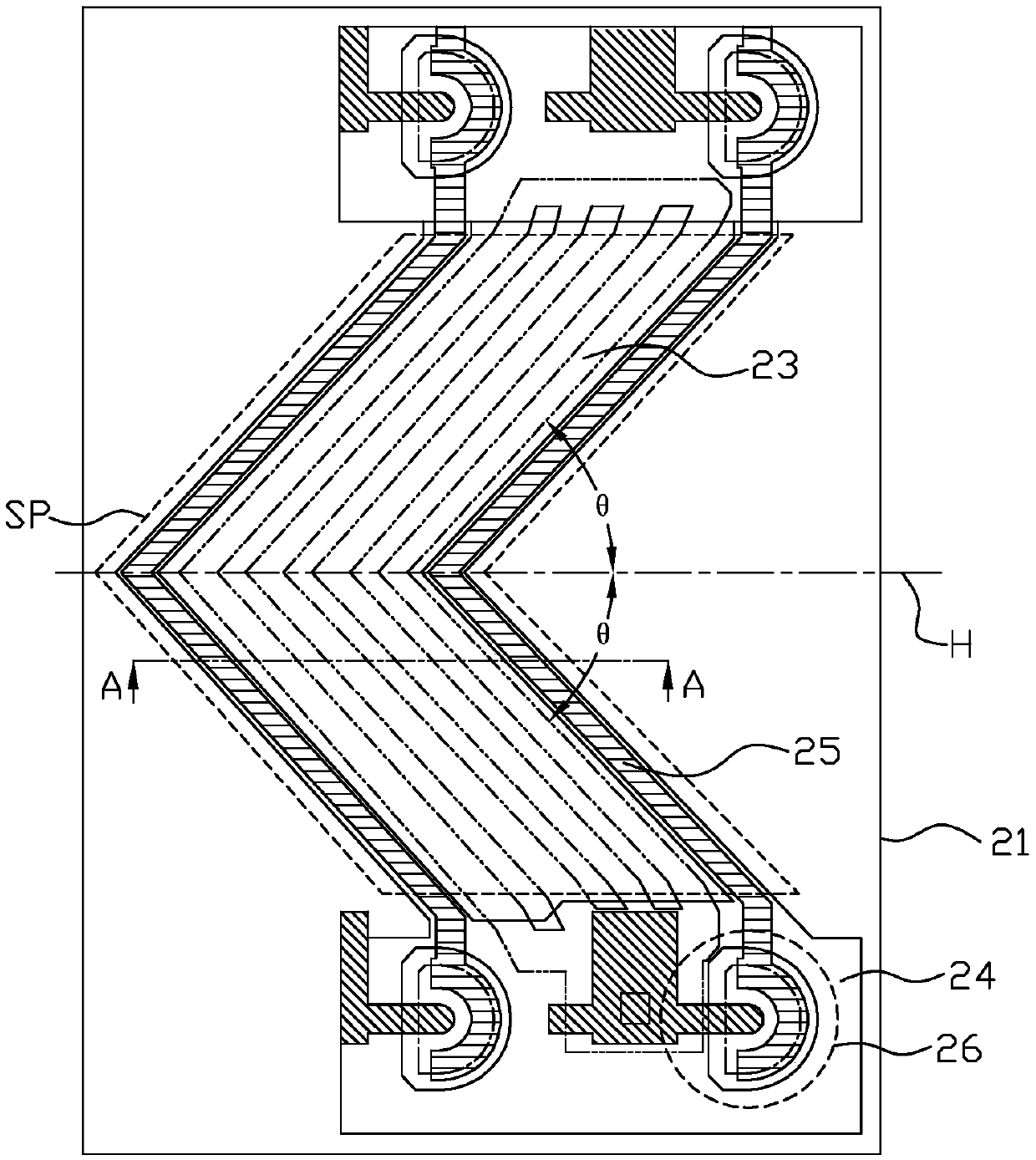
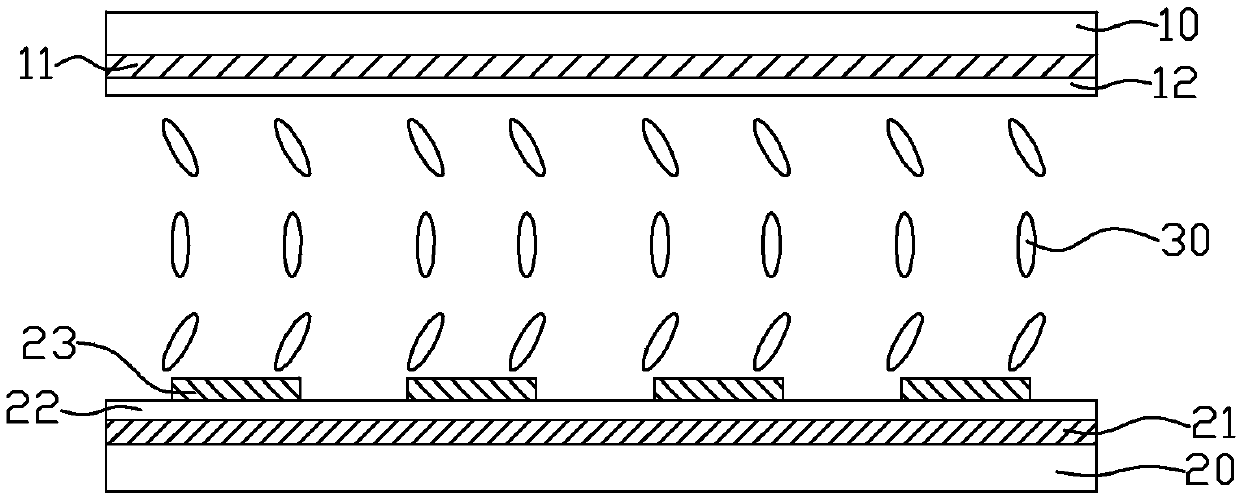
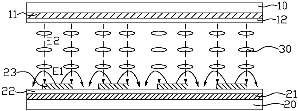
[0029] Such as Figure 1 to Figure 4 As shown, a liquid crystal display panel provided by the present invention includes a first substrate 10 , a second substrate 20 opposite to the first substrate 10 , and a liquid crystal layer 30 between the first substrate 10 and the second substrate 20 . The first substrate 10 can be a substrate made of glass, acrylic, polycarbonate and other materials. In this embodiment, the first substrate 10 is a glass substrate, and the second substrate 20 is a thin film transistor array substrate. The liquid crystal layer 30 adopts positive liquid crystal molecules, that is, liquid crystal molecules with positive dielectric anisotropy, and the positive liquid crystal molecules adopt vertical alignment (that is, the long axis of the positive liquid crystal molecules is 70°-90° to the first substrate 10 ), In this embodiment, the initial state of the positive liquid crystal molecules is perpendicular to the first substrate 10 and the second substrate ...

Embodiment 2

[0040] Such as Figure 6 As shown, the liquid crystal display panel provided by Embodiment 2 of the present invention is the same as Embodiment 1 ( figure 1 ) in the structure and working principle of the liquid crystal display panel are basically the same, the difference is that, in this embodiment, each pixel electrode 23 is a ">" shape structure, which is the pixel with a "<" shape structure in the first embodiment The directions of the electrodes 23 are reversed, so that multiple implementations can be selected while achieving the purpose of the present invention.

[0041] Those skilled in the art should understand that the remaining structures and working principles of this embodiment are the same as those of Embodiment 1, and will not be repeated here.

Embodiment 3

[0043] Such as Figure 7 and Figure 8 As shown, the liquid crystal display panel provided by Embodiment 3 of the present invention is the same as Embodiment 1 ( figure 1 and Figure 4 ) in the liquid crystal display panel are basically the same in structure and working principle, the difference is that in this embodiment, the auxiliary electrode 11 is a planar structure arranged on the entire surface, and the common electrode 21 and the pixel electrode 23 are all with slits Comb structure, so that multiple implementation options are available while realizing the purpose of the present invention.

[0044] Those skilled in the art should understand that the remaining structures and working principles of this embodiment are the same as those of Embodiment 1, and will not be repeated here.


PUM


Abstract

The invention discloses a liquid crystal display panel comprising a first substrate, a second substrate and a liquid crystal layer arranged between the first substrate and the second substrate. An auxiliary electrode is arranged on the first substrate. A common electrode and a plurality of sub pixels arranged in an array are arranged on the second substrate; and a pixel electrode is arranged in each sub pixel. The liquid crystal layer employs positive liquid crystal molecules; and the initial state of the positive liquid crystal molecule is a state being perpendicular to the first substrate and the second substrate. Each pixel electrode has a < type or > type structure; a value range of an angle theta between an electrode bar of each pixel electrode and a horizontal direction is from 30 degrees to 83 degrees. The common electrode is used for applying a direct-current common voltage; the auxiliary electrode is used for applying an auxiliary reference voltage; and the potential of the auxiliary reference voltage is not equal to that of the direct-current common voltage and a voltage difference between the auxiliary electrode and the common electrode is larger than a preset value. Inaddition, the invention also discloses a liquid crystal display device including the liquid crystal display panel.

Description

technical field [0001] The invention relates to the technical field of liquid crystal display, in particular to a liquid crystal display panel and a liquid crystal display device. Background technique [0002] The response time of the liquid crystal display panel consists of a rise time and a fall time. The rise time refers to the time required for the LCD panel to complete the liquid crystal deflection from the black state display to the white state display. The fall time refers to the liquid crystal display panel. The time required for liquid crystal deflection to complete the process of changing from white state display to black state display. Among them, black state display is also called dark state display, at this time, the deflected liquid crystal does not allow light to pass through; white state display is also called bright state display, at this time, the deflected liquid crystal allows light to pass through to the greatest extent. [0003] FSC (Field Sequential C...

Claims


Application Information

Patent Timeline
Patent Type & Authority Applications(China)
IPC IPC(8): G02F1/137G02F1/1343G02F1/1333
CPCG02F1/133345G02F1/134309G02F1/134363G02F1/137G02F1/134381G02F1/13706
Inventor 钟德镇苏子芳李冬敏
Owner KUSN INFOVISION OPTOELECTRONICS
Why Eureka
Try Eureka